Charge pump circuit

A charge pump and circuit technology, applied in the direction of conversion equipment without intermediate conversion to AC, can solve the problems of unstable memory operation, affecting the stability of data writing, device reliability, etc., to reduce the boosting speed and reduce the range Effect

Active Publication Date: 2011-09-21
SHANGHAI HUAHONG GRACE SEMICON MFG CORP
View PDF6 Cites 7 Cited by
  • Summary
  • Abstract
  • Description
  • Claims
  • Application Information

AI Technical Summary

Problems solved by technology

The periodic change of the output voltage of the charge pump circuit is called "ripple". If the voltage amplitude of the ripple changes

Method used


Image

  • Charge pump circuit
  • Charge pump circuit
  • Charge pump circuit

Examples


Embodiment Construction

[0023] In order to make the above objects, features and advantages of the present invention more comprehensible, specific implementations of the present invention will be described in detail below in conjunction with the accompanying drawings.

[0024] In the following description, many specific details are set forth in order to fully understand the present invention, but the present invention can also be implemented in other ways than those described here, so the present invention is not limited by the specific embodiments disclosed below.

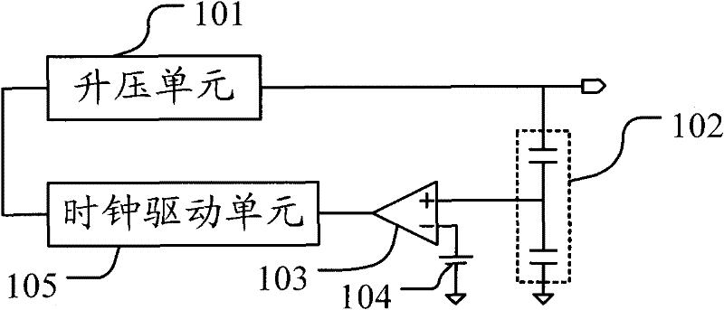
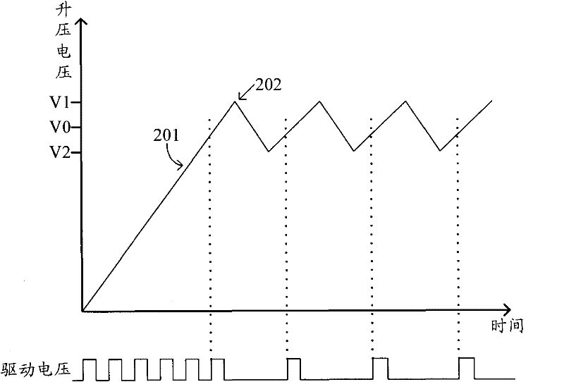
[0025] As described in the background technology section, in the charge pump circuit, due to the path delay in the path from the voltage comparison unit to the input terminal of the boost unit, the boosted voltage output by the boost unit will temporarily exceed the target voltage, resulting in an overshoot phenomenon; The overshoot phenomenon makes the output voltage of the charge pump circuit fluctuate periodically.

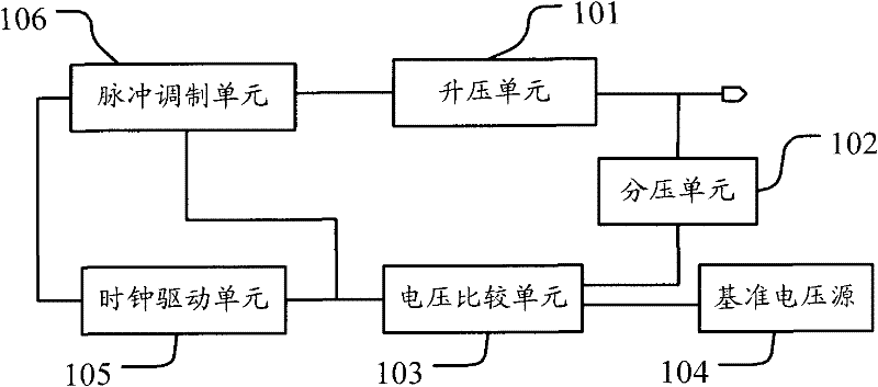
[0026] The boost u...


PUM


Abstract

The invention relates to a charge pump circuit which comprises a boosting unit, a voltage division unit, a reference voltage source, a voltage comparison unit, a timepiece driver unit and an impulse modulation unit, wherein, the boosting unit is used for promoting the boosting voltage according to a modulation voltage output by the impulse modulation unit; the voltage division unit is used for carrying out voltage division on the boosting voltage output by the boosting unit and outputting the divided voltage; the voltage comparison unit is used for comparing the divided voltage with the reference voltage so as to provide a control voltage to the timepiece driver unit and the impulse modulation unit according to the comparison result; the timepiece driver unit is used for receiving the control voltage output by the voltage comparison unit, forming a driving voltage based on the control voltage and sending to the impulse modulation unit; and the impulse modulation unit is used for modulating the driving voltage sent by the timepiece driver unit according to the control voltage and sending a modulation voltage to the boosting unit.

Description

technical field [0001] The present invention relates to the field of semiconductor technology, and more particularly, the present invention relates to a charge pump circuit. Background technique [0002] In recent years, in the process of rapid development of semiconductor memory, due to the advantages of high density, low power consumption and low price of advanced memory such as DRAM, EEPROM, FLASH, it has become a storage device commonly used in computers and mobile communication terminals. [0003] In semiconductor memory, the charge pump circuit is a circuit module that provides high voltage, and the storage system uses the high-amplitude programming voltage output by the charge pump circuit to write data information into the memory module. The Japanese patent No. JP2004-259405 discloses a charge pump circuit, the schematic diagram of which is shown in figure 1 As shown, it includes: a boost unit 101, a voltage divider 102, a voltage comparison unit 103, a reference vo...

Claims


Application Information

Patent Timeline
IPC IPC(8): H02M3/07
Inventor 杨光军
Owner SHANGHAI HUAHONG GRACE SEMICON MFG CORP
Why Eureka
Try Eureka