Light-emitting diode (LED) multi-chip integrated packaging device

An integrated packaging and multi-chip technology, applied in the direction of electric solid-state devices, semiconductor devices, electrical components, etc., can solve the problems of reduced life, low reliability, and low luminous efficiency, and achieve increased reliability, improved light efficiency, and long service life. prolonged effect

Inactive Publication Date: 2011-09-28
安徽莱德电子科技有限公司
View PDF0 Cites 0 Cited by
  • Summary
  • Abstract
  • Description
  • Claims
  • Application Information

AI Technical Summary

Problems solved by technology

[0003] The purpose of the present invention is to solve the problems of large thermal resistance, low reliability, low luminous efficiency, difficult secondary heat dissipation treatment of the device, and reduced service life of the existing LED multi-chip integrated packaging device.

Method used


Image

  • Light-emitting diode (LED) multi-chip integrated packaging device
  • Light-emitting diode (LED) multi-chip integrated packaging device

Examples


Embodiment Construction

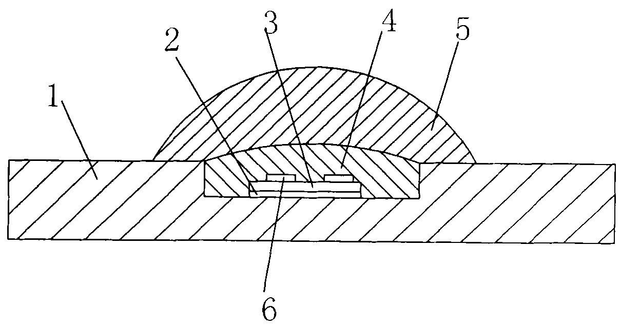
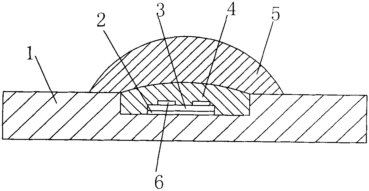
[0009] A kind of LED multi-chip integrated packaging device of the present invention, as figure 1 As shown, it includes a substrate 1 and several chips 6, and it also includes a silicon chip 3, a phosphor layer 4 and an optical silicone lens 5. The bottom of the silicon chip 3 is plated with a gold-plated layer, and several chips 6 are welded in series and parallel on the silicon chip. A series-parallel circuit is formed on the chip 3, the substrate 1 is a red copper plate, a square groove is opened on the substrate 1, the bottom of the square groove is electroplated with nickel silver, the silicon chip 3 is located in the square groove, and an alloy is formed between the silicon chip 3 and the bottom of the square groove. The soldering piece 2 fixes the silicon chip 3 in the square groove; the phosphor layer 4 fills and covers the silicon chip 3 and forms a convex surface on the upper surface, and the silicone lens 5 is fixed on the substrate 1 in a hemispherical shape to cove...


PUM


Abstract

The invention discloses a light-emitting diode (LED) multi-chip integrated packaging device, which comprises a substrate [1] and a plurality of chips [6], and is characterized by also comprising a silicon chip [3], a fluorescent powder layer [4] and an optical silica gel lens [5], wherein a gold-plating layer is plated at the bottom of the silicon chip [3]; the plurality of chips [6] are welded on the silicon chip [3] in parallel and in series so as to form a serial/parallel circuit; the substrate [1] is a red copper plate; a square groove is formed on the substrate [1]; nickel silver is electroplated at the bottom of the square groove; the silicon chip [3] is positioned in the square groove; an alloy soldering lug [2] is arranged between the silicon chip [3] and the bottom of the square groove, so that the silicon chip [3] is fixed in the square groove; the fluorescent powder layer [4] is filled in and covers the silicon chip [3] and a convex surface is formed on an upper surface of the fluorescent powder layer [4]; and the silica gel lens [5] is hemispherically fixed on the substrate [1] and covers the fluorescent powder layer [4]. The LED multi-chip integrated packaging device has the advantages of high reliability, high luminous efficiency and long service life.

Description

technical field [0001] The invention relates to an LED multi-chip integrated packaging device. Background technique [0002] Existing LED multi-chip integrated packaging devices mostly use multiple small chips or multiple large chips to be integrated in series and parallel; the substrate mostly uses an aluminum-based circuit board; the chip and the substrate are bonded with silver glue; In the way of circular grooves, yellow fluorescent glue is filled in the middle to form white light. For most of the current packaging forms of LED integrated packaging devices, the LED devices have disadvantages such as large packaging thermal resistance, reduced reliability, low luminous efficiency, difficult secondary heat dissipation treatment of the device, and reduced lifespan. Contents of the invention [0003] The purpose of the present invention is to solve the problems of large thermal resistance, low reliability, low luminous efficiency, difficult secondary heat dissipation trea...

Claims


Application Information

Patent Timeline
Patent Type & Authority Applications(China)
IPC IPC(8): H01L25/075H01L33/48H01L33/62
Inventor 向德祥于正国李静静徐俊峰
Owner 安徽莱德电子科技有限公司
Why Eureka
Try Eureka