Manufacturing method of electronic parts module

An electronic component and manufacturing method technology, applied in the field of electronic component module manufacturing, can solve the problems of inability to prevent electric field noise and electromagnetic noise, achieve the effects of thinning and miniaturization, improving production efficiency, and reducing substrate area

Active Publication Date: 2013-07-31
MURATA MFG CO LTD
View PDF4 Cites 1 Cited by
  • Summary
  • Abstract
  • Description
  • Claims
  • Application Information

AI Technical Summary

Problems solved by technology

[0003] However, since the electronic component module manufactured and cut out by the manufacturing method disclosed in Patent Document 1 has no shielding layer formed on the side surface, it is impossible to prevent electric field noise and electromagnetic noise from entering from the side surface.

Method used


Image

  • Manufacturing method of electronic parts module
  • Manufacturing method of electronic parts module
  • Manufacturing method of electronic parts module

Examples


Embodiment approach 1

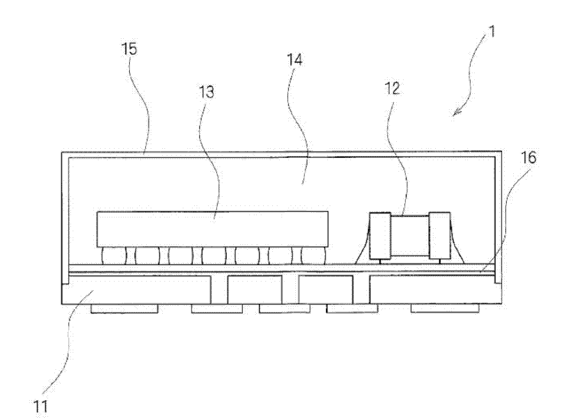
[0069] figure 1 It is a cross-sectional view showing the configuration of the electronic component module according to Embodiment 1 of the present invention. The electronic component module 1 according to Embodiment 1 of the present invention has, for example, a rectangular parallelepiped shape of 10.0 mm×10.0 mm×1.2 mm, and includes: a circuit board 11 made of ceramics, glass, epoxy resin, etc.; Electronic components 12, 12, ..., 13, 13, ... such as semiconductor elements on the surface, capacitors, resistors, and SAW filters.

[0070] The circuit board 11 is, for example, a resin substrate having a rectangular upper surface and a thickness of 0.5 mm. The surface of the circuit board 11 is provided with a signal pattern (not shown) serving as a bonding pad (electrode pad) between the electronic components 12, 12, ..., 13, 13, ... and a ground electrode on the side wall of the circuit board 11. 16. The signal pattern of the circuit board 11 is connected to terminals of ele...

Embodiment approach 2

[0087] Since the configuration of the electronic component module according to Embodiment 2 of the present invention and figure 1 The configuration of the electronic component module 1 according to Embodiment 1 shown is the same, and therefore the same reference numerals are used to omit detailed description.

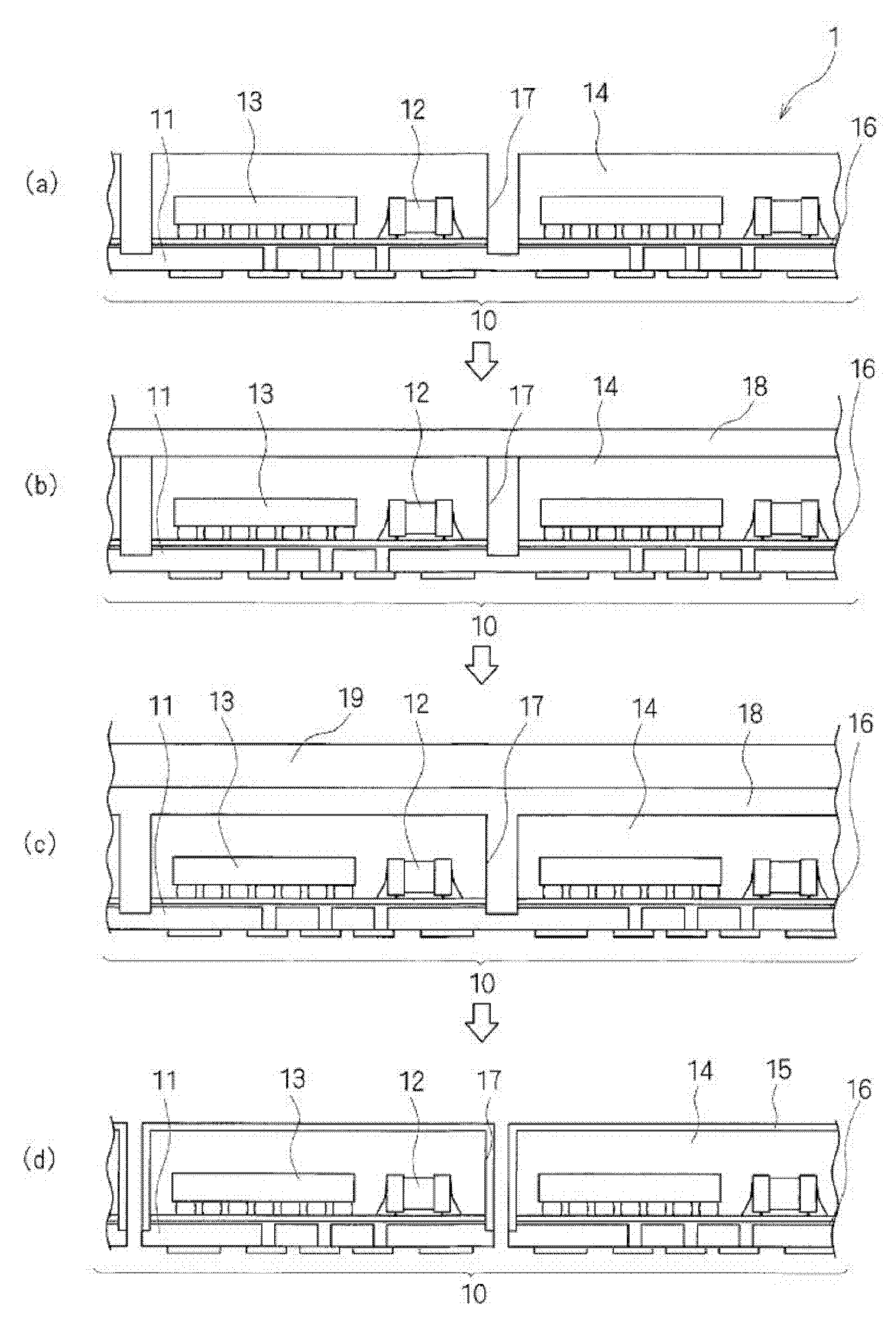
[0088] Figure 4 It is a sectional view explaining the manufacturing method of the electronic component module 1 which concerns on Embodiment 2 of this invention. Figure 4 (a) shows the state where the notch part 17 was formed after the sealing resin layer 14 was formed, Figure 4 (b) shows the state where the sheet-shaped conductive resin 18 is set, Figure 4 (c) shows the state where the collective substrate 10 is pressurized and heated by the pressure furnace device 21, Figure 4 (d) shows the state where the shielding layer 15 is formed. in addition, Figure 4 (a) and (b) of figure 2 (a) and (b) are the same.

[0089] As in Embodiment 1, the insulating lay...

Embodiment approach 3

[0097] Since the configuration of the electronic component module according to Embodiment 3 of the present invention and figure 1 The configuration of the electronic component module 1 according to Embodiment 1 shown is the same, and therefore the same reference numerals are used to omit detailed description.

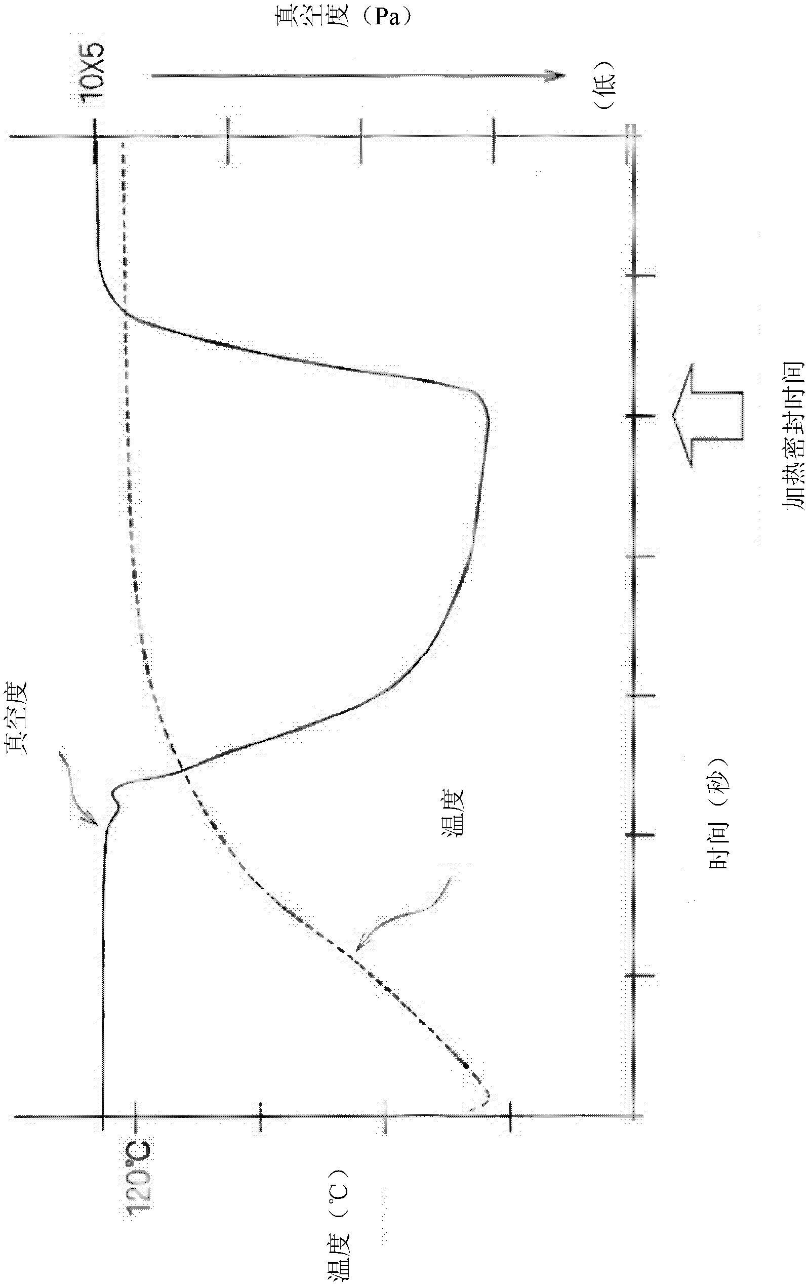
[0098] Figure 5 It is a sectional view explaining the manufacturing method of the electronic component module 1 which concerns on Embodiment 3 of this invention. Figure 5 (a) It is the state which formed the notch part 17 after forming the sealing resin layer 14, Figure 5 (b) shows the state where the sheet-shaped conductive resin 18 is set, Figure 5 (c) shows the state where the collective substrate 10 is placed in a gas-insulating bag 22 and decompressed, Figure 5 (d) shows the state where the aggregated substrate 10 in the depressurized bag 22 is heated. in addition, Figure 5 (a) and (b) of figure 2 (a) and (b) are the same.

[0099] As in Embodiment 1...


PUM

PropertyMeasurementUnit
thicknessaaaaaaaaaa
thicknessaaaaaaaaaa

Abstract

Provided is a manufacturing method of an electronic parts module which can reliably shield electronic parts and implement a compact size. An assembly board (10) forming a plurality of electronic parts modules (1) from a plurality of electronic parts (12,13) is sealed as a whole by resin. Notches (17) are formed from the top surface of the sealed sealing resin layer (14) at the boundaries of the electronic parts modules (1) to positions which reach the ground electrode (16) provided inside of the assembly board (10). After a conductive resin (18) sheet is positioned to cover the notches (17) and the top surface, the conductive resin (18) fills in the notches (17) and connects to the ground electrode (16) by applying pressure and heating the assembly board (10) with the conductive resin (18) sheet placed thereon.

Description

technical field [0001] The present invention relates to a method of manufacturing an electronic component module. The method involves cutting out an electronic component module having a ground electrode inside the composite substrate from a composite substrate in which a plurality of electronic component modules are formed by a plurality of electronic components. Background technique [0002] In the past, when manufacturing electronic component modules, for example, on the substrate on which the electronic components are placed, a ground terminal of a predetermined height is provided, and a laminated sheet made of a resin film and a conductive film having a shielding effect is arranged on the substrate. , by softening the resin film, the ground terminal communicates with the conductive film (refer to Patent Document 1). [0003] However, since the electronic component module manufactured and cut out by the manufacturing method disclosed in Patent Document 1 has no shielding ...

Claims


Application Information

Patent Timeline
Patent Type & Authority Patents(China)
IPC IPC(8): H01L21/56H01L23/00H01L23/28
CPCH05K1/0218H01L2924/01002H01L2224/97H01L2924/01047H01L2924/3025H01L2924/014H01L24/97H01L23/552H01L2924/01029H01L2924/09701H05K3/284H05K2201/0129H01L2924/01005H01L2924/01033H01L25/165H01L2924/01004H01L23/3121H01L2924/19041H01L21/56H05K2203/0278H05K2203/1105H01L2924/01006H05K3/0052H01L2224/16225H01L2924/19105H01L2924/181
Inventor 神凉康一胜部彰夫北村俊辅片冈祐治
Owner MURATA MFG CO LTD
Why Eureka
Try Eureka