Temperature compensation attenuator
A technology of temperature compensation and attenuator, which is applied in waveguide devices, electrical components, circuits, etc., can solve the problem of unfriendly environment, parasitic capacitive reactance affecting high-frequency performance of devices, process and performance controllability, repeatability and consistency Low-level problems, to achieve the effect of thin film and serialization
- Summary
- Abstract
- Description
- Claims
- Application Information
AI Technical Summary
Problems solved by technology
Method used
Image
Examples
Embodiment 1
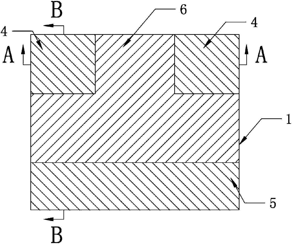
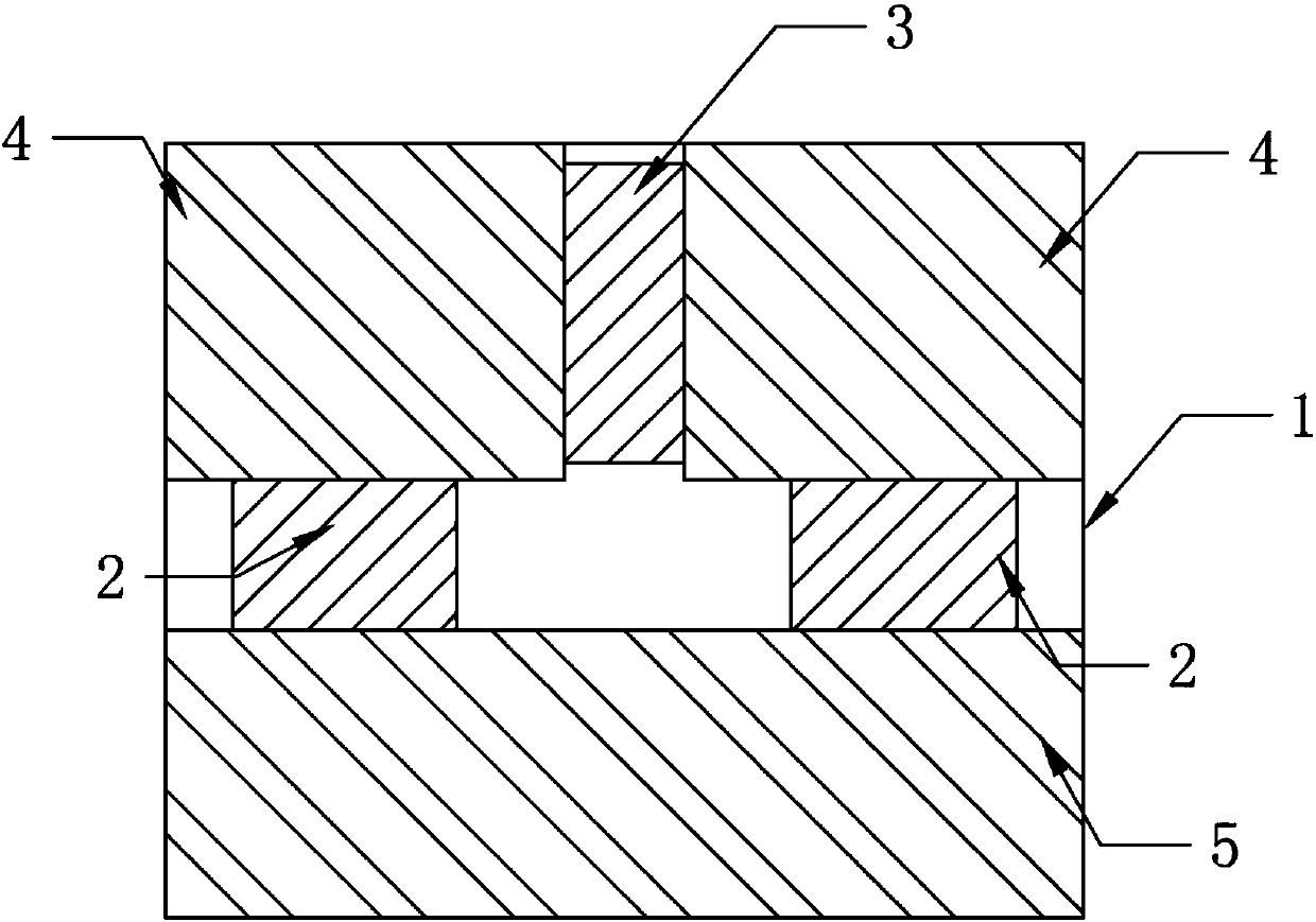
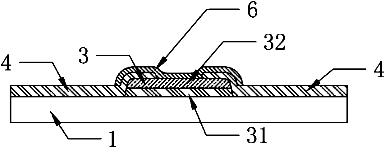
[0037] like figure 2 As shown, a temperature compensation attenuator according to an embodiment of the present invention includes a substrate 1 on which a first thermistor 2, a second thermistor 3, a signal electrode 4 and a ground electrode 5 are arranged. A thermistor 2 is a thin film PTC thermistor; as image 3 As shown, the second thermistor 3 is formed by stacking a conductive layer 31 and a thin film NTC thermistor 32, and the conductive layer 31 is arranged between the substrate 1 and the thin film NTC thermistor 32; figure 2 , image 3 and Figure 4 As shown, the signal electrode 4 is electrically connected to the first thermistor 2 and the thin film NTC thermistor 32 respectively, and the ground electrode 5 is electrically connected to the first thermistor 2 or the thin film NTC thermistor 32 .
[0038] In the above structure, the thin film NTC thermistor R in the two thickness directions 2 , R 3 and the resistance of the conductive layer R 4 form a series str...
Embodiment 2
[0048] A temperature-compensated attenuator in the embodiment of the present invention differs from the temperature-compensated attenuator in Embodiment 1 only in that in this embodiment, the material of the conductive layer 31 is an oxide, and the resistivity of the conductive layer 31 is related to the NTC heat of the thin film. The ratio of the resistivity of the sensitive resistor 32 is 3×10 -5 ~7×10 -4 between. The oxide can be a binary oxide conductive material and some composite oxide conductive materials with a perovskite structure, and the oxide must have high temperature resistance. At this time, the resistance of the conductive layer is large and the TCR is small, the resistance of the thin film NTC thermistor is small and the value of B is large, and the conductive layer and the thin film NTC thermistor form a series structure, so as to realize the total resistance R and equal Thin film NTC thermistor with small effective B value. Figure 13 It is a typical resi...
Embodiment 3
[0051] A temperature compensation attenuator according to an embodiment of the present invention differs from the temperature compensation attenuator in Embodiment 1 only in that in this embodiment, the second thermistor consists of two layers of conductive layers and two layers of thin film NTC thermistors alternately stacked, and the bottom conductive layer is arranged between the substrate and the bottom thin film NTC thermistor.
[0052] In this embodiment, the thicknesses of the conductive layer and the thin-film NTC thermistor in Embodiment 1 are halved, and the number of layers is doubled for alternate deposition to form a four-layer stacked structure, while other structural dimensions remain unchanged. The resistance temperature characteristics of the total resistance of the four-layer stacked NTC thermistor are as follows Image 6 shown. Compared Figure 13 and Image 6 It can be seen that the total resistance value of the four-layer stacked structure can be reduce...
PUM
 Abstract
Description
Claims
Application Information


