Terminal structure of power semiconductor device and power semiconductor device

A technology of power semiconductor and terminal structure, applied in the direction of semiconductor devices, electrical components, circuits, etc., can solve the problems of not reaching the maximum withstand voltage, limiting the axial withstand voltage capacity of power semiconductors, etc., so as to reduce the hold-up and improve the breakdown voltage. Effect

Active Publication Date: 2011-10-05
BYD SEMICON CO LTD
View PDF4 Cites 1 Cited by
  • Summary
  • Abstract
  • Description
  • Claims
  • Application Information

AI Technical Summary

Problems solved by technology

from Figure 2B We can get that the electric field curve of the depletion layer has multiple peaks and troughs, so its withstand voltage does not reach the maximum, which limits the axial withstand voltage capability of the power semiconductor

Method used


Image

  • Terminal structure of power semiconductor device and power semiconductor device
  • Terminal structure of power semiconductor device and power semiconductor device
  • Terminal structure of power semiconductor device and power semiconductor device

Examples


Embodiment Construction

[0012] In order to make the technical problems, technical solutions and beneficial effects solved by the present invention clearer, the following further describes the present invention in detail with reference to the accompanying drawings and embodiments. It should be understood that the specific embodiments described herein are only used to explain the present invention, but not to limit the present invention.

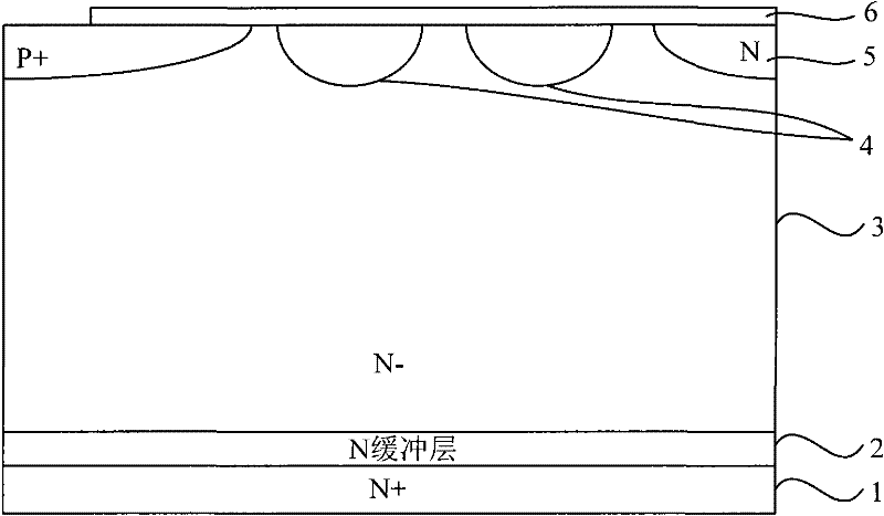
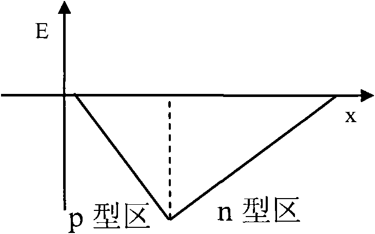
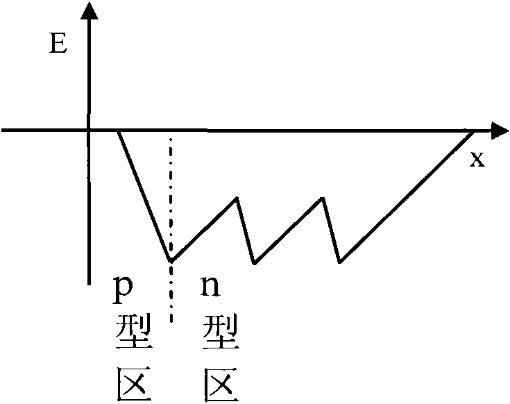
[0013] Before describing the embodiments of the present invention in detail, the breakdown mechanism of the electric field confinement ring (field ring) will be described first. The electric field limit ring generally uses the electric field valley generated by the depletion of the p-type region to offset the superimposed influence of the electric field peak generated by the depletion of the n-type region on the maximum electric field value, so as to achieve the purpose of withstand voltage. The breakdown of the electric field confinement ring means the breakdown of the...


PUM


Abstract

The invention provides a terminal structure of a power semiconductor device and a power semiconductor device. The terminal structure of the power semiconductor device comprises a channel ring in the main body semiconductor area of the power semiconductor device, wherein the material of the channel ring is intrinsic polycrystalline material whose relative dielectric constant is a value from 1 to 15, and the intrinsic polycrystalline material is intrinsic polycrystalline silicon carbide. In the invention, the intrinsic polycrystalline silicon carbide with relative dielectric constant within15 is used in the channel ring in the terminal structure of the power semiconductor device. Thus electric field line which goes through the channel ring area is nearly level. There is no extreme point in the area. The carrier hold-up is substantially reduced. Thereby breakdown voltage is raised.

Description

Technical field [0001] The invention belongs to the technical field of semiconductor device protection, and in particular relates to a terminal structure of a power semiconductor device and a power semiconductor device. Background technique [0002] The electric field confinement ring, referred to as the field ring, is one of the commonly used terminals of power semiconductor devices. The application of the field ring can improve the fringe electric field distribution of the power semiconductor device, and improve the voltage resistance and stability of the power semiconductor device. figure 1 It is a schematic diagram of the terminal structure of an existing power semiconductor device. Please refer to figure 1 , The power semiconductor device includes a heavily doped N-type substrate 1 (N+ substrate 1), an N-type buffer layer 2 on the N+ substrate 1, a lightly doped N-type epitaxial layer 3 on the N-type buffer layer 2 (N-type epitaxial layer 3) and functional regions and prote...

Claims


Application Information

Patent Timeline
Patent Type & Authority Applications(China)
IPC IPC(8): H01L29/06H01L29/12
Inventor 周振强江堂华吴家键蔡桥斌
Owner BYD SEMICON CO LTD
Why Eureka
Try Eureka