Semiconductor device and method for manufacturing the semiconductor device

A manufacturing method and semiconductor technology, applied in the fields of semiconductor/solid-state device manufacturing, semiconductor devices, electrical components, etc., can solve the problems of changing circuit constants, parasitic oscillation, etc., and achieve reduced ON impedance, good withstand voltage characteristics, and difficult gate parasitic oscillation. Effect

Active Publication Date: 2011-10-05
SHINDENGEN ELECTRIC MFG CO LTD
View PDF5 Cites 5 Cited by
  • Summary
  • Abstract
  • Description
  • Claims
  • Application Information

AI Technical Summary

Problems solved by technology

[0011] However, in the conventional semiconductor device 90, although it is possible to miniaturize the semiconductor device without increasing the ON resistance of the semiconductor device, the switching speed (Switching Speed) becomes fast, so that the circuit is cut off under certain usage conditions. When the parasitic oscillation of the gate is easy to occur, in order to suppress this parasitic oscillation, it may be necessary to change the circuit constant

Method used


Image

  • Semiconductor device and method for manufacturing the semiconductor device
  • Semiconductor device and method for manufacturing the semiconductor device
  • Semiconductor device and method for manufacturing the semiconductor device

Examples


Embodiment Construction

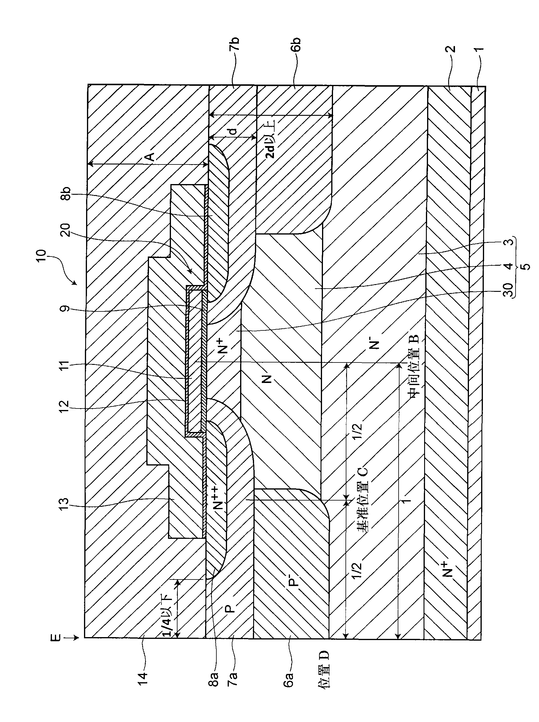
[0059] Hereinafter, the semiconductor device and the manufacturing method of the semiconductor device according to the present invention will be described in detail with reference to the drawings.

[0060] 1. Structure of semiconductor device 10

[0061] figure 1 It is a sectional view showing the semiconductor device 10 in the embodiment.

[0062] The semiconductor device 10 in the embodiment is a MOSFET (Field Effect Transistor) whose current is controlled by a voltage applied to a gate electrode. The MOSFET has a structure of a plurality of MOSFETs arranged in parallel. In addition, since each MOSFET arranged in parallel has the same structure, in this embodiment, only the structure of one MOSFET is demonstrated as a representative example.

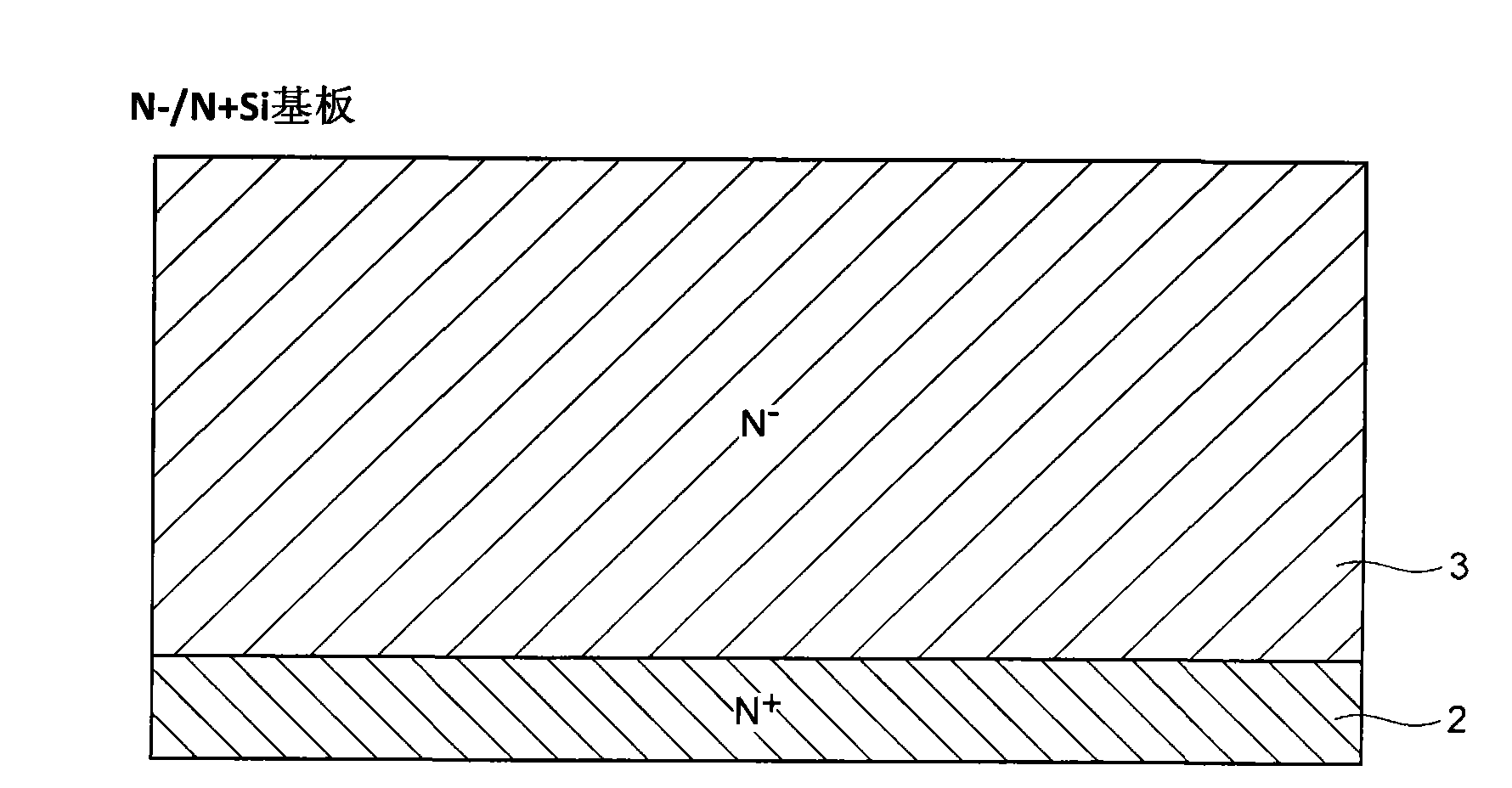
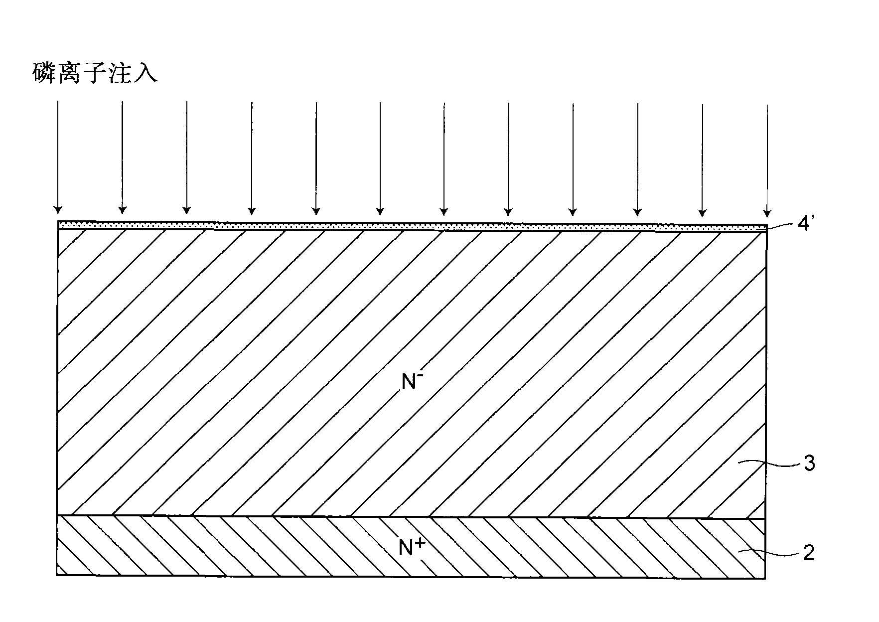
[0063] Such as figure 1 As shown, the semiconductor device 10 in the embodiment has a reference concentration layer 4 containing an n-type impurity of the first conductivity type at a predetermined first reference concentration an...


PUM


Abstract

A semiconductor device which can make the generation of gate parasitic oscillations more difficult than a semiconductor device of the related art is provided. The semiconductor device 10 includes: a drift layer 15 which is constituted of a reference concentration layer 4 and a low concentration layer 3; a gate electrode structure 20; a pair of source regions 8a 8b, a pair of base regions 7a 7b, and depletion-layer extension regions 6a 6b which are formed in the reference concentration layer below the base regions 7a 7b, wherein the depletion-layer extension regions 6a 6b are formed such that a lower surface of the depletion-layer extension region is deeper than a boundary between the low concentration layer 3 and the reference concentration layer 4 and projects into the low concentration layers 3, and a dVDS / dt-decreasing diffusion layer 30 which contains an n-type impurity at a concentration higher than the concentration of the impurity which the reference concentration layer 4 contains and decreases dVDS / dt when the semiconductor device is turned off is formed on a surface of the reference concentration layer 4.

Description

technical field [0001] The present invention relates to a semiconductor device and a manufacturing method thereof. Background technique [0002] Conventionally, there is a semiconductor device that can be miniaturized without increasing the ON resistance of the semiconductor device and has good withstand voltage characteristics (for example, refer to Patent Document 1). Figure 8 It is a sectional view of such a conventional semiconductor device 90 . [0003] The conventional semiconductor device 90 is a power MOSFET such as Figure 8 As shown, it has: a reference concentration layer 4 containing an n-type impurity (first conductivity type impurity) of the first reference concentration and an n-type impurity lower than the first reference concentration provided on the lower surface of the reference concentration layer 4 Drift layer 5 made of low concentration layer 3, the gate electrode (polysilicon layer 11 of gate electrode structure 20) formed by gate insulating film 9 on...

Claims


Application Information

Patent Timeline
Patent Type & Authority Applications(China)
IPC IPC(8): H01L29/06H01L29/78H01L29/739H01L21/265H01L21/336H01L21/331
CPCH01L29/66712H01L29/1095H01L29/0878H01L29/0634H01L29/7802H01L29/7395H01L29/47
Inventor 渡边祐司福井正纪丸冈道明
Owner SHINDENGEN ELECTRIC MFG CO LTD
Why Eureka
Try Eureka