mosfet and power conversion circuit
A power conversion circuit and current technology, applied in circuits, output power conversion devices, electrical components, etc., can solve problems such as MOSFET oscillation and surge voltage of rectifier components
- Summary
- Abstract
- Description
- Claims
- Application Information
AI Technical Summary
Problems solved by technology
Method used
Image

Examples
Embodiment approach 1
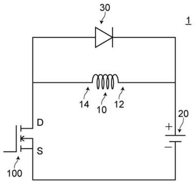
[0049] 1. Configuration and operation of the power conversion circuit 1 according to the first embodiment
[0050] The power conversion circuit 1 according to the first embodiment is a chopper circuit as a component such as a DC-DC converter or an inverter. The power conversion circuit 1 related to the first embodiment is as figure 1 As shown, it includes: a reactor 10 ; a power supply 20 ; a MOSFET 100 ; and a rectifying element 30 . MOSFET 100 is MOSFET 100 according to the first embodiment.
[0051] The reactor 10 is a passive element capable of storing energy in a magnetic field formed by passing an electric current.
[0052] The power source 20 is a DC power source that supplies current to the reactor 10 .
[0053] MOSFET 100 controls the current supplied to reactor 10 by power supply 20 . Specifically, the MOSFET 100 switches and switches in response to a signal (such as a clock signal) applied to the gate electrode of the MOSFET 100 by a driving circuit (not shown)...
Embodiment approach 2
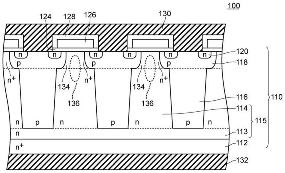
[0121] MOSFET 102 according to Embodiment 2 basically has the same configuration as MOSFET 100 according to Embodiment 1, but differs from MOSFET 100 according to Embodiment 1 in that it is a trench gate MOSFET rather than a planar gate MOSFET. That is, the MOSFET 102 involved in the second embodiment is as Figure 12 As shown, the semiconductor substrate 110 has: a p-type base region 118 formed on the surfaces of the n-type columnar region 114 and the p-type columnar region 116; and an n-type source region 120 formed on the surface of the base region 118 , the MOSFET 102 involved in Embodiment 2 is a trench gate MOSFET, which further includes: in the area where the n-type columnar region 114 is located, it is formed to a position deeper than the deepest part of the base region 118 when viewed from a plane and is formed such that a part of the source region 120 is exposed on the inner peripheral surface of the trench 138; and is buried inside the trench 138 via the gate insula...
Embodiment approach 3
[0128] The power conversion circuit 4 according to the third embodiment basically has the same configuration as the power conversion circuit 1 according to the first embodiment, but is different from the power conversion circuit 1 according to the first embodiment in that it is a full bridge circuit. That is, the power conversion circuit 4 related to the third embodiment is as Figure 13 As shown, four MOSFETs 100 are provided as MOSFETs, and built-in diodes of each MOSFET are provided as rectifying elements.
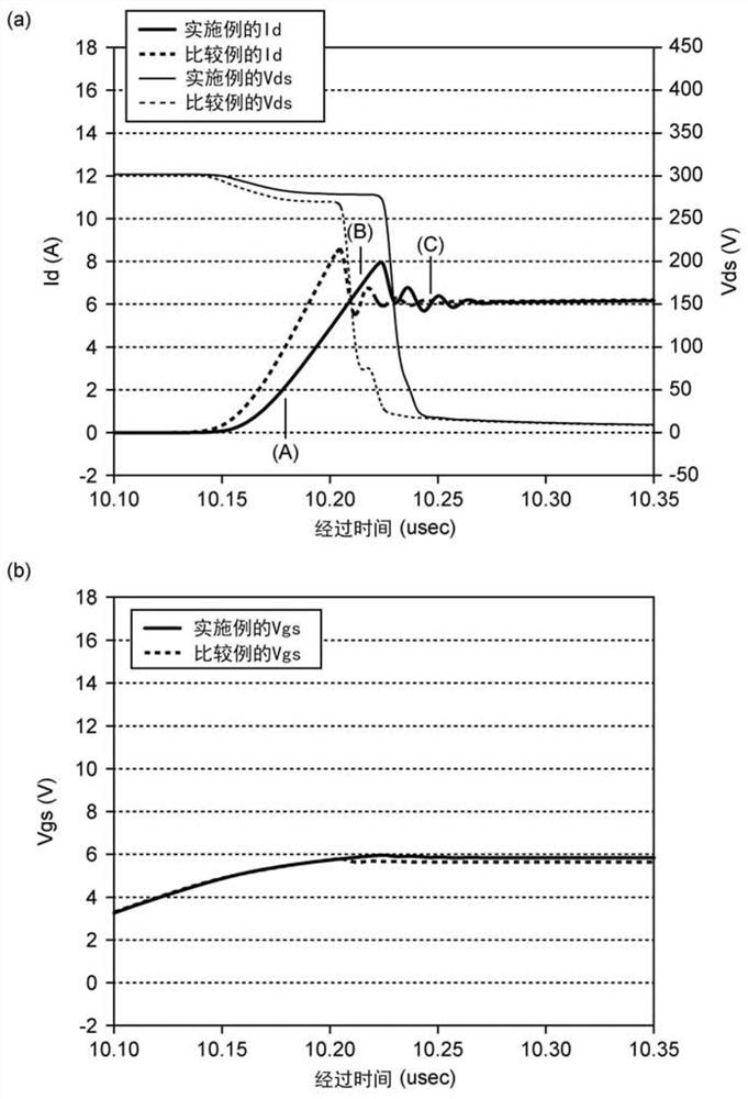
[0129] In this way, although the power conversion circuit 4 according to the third embodiment is different from the power conversion circuit 1 according to the first embodiment in that it is a full bridge circuit, like the power conversion circuit 1 according to the first embodiment, since the MOSFET Finally, the operation is as follows: in the center of the n-type columnar region 114, a low-electric-field region 136 with an electric field intensity lower than that of t...
PUM
| Property | Measurement | Unit |
|---|---|---|
| thickness | aaaaa | aaaaa |
| thickness | aaaaa | aaaaa |
| thickness | aaaaa | aaaaa |
Abstract
Description
Claims
Application Information
 - R&D
- Intellectual Property
- Life Sciences
- Materials
- Tech Scout
- Unparalleled Data Quality
- Higher Quality Content
- 60% Fewer Hallucinations
Browse by: Latest US Patents, China's latest patents, Technical Efficacy Thesaurus, Application Domain, Technology Topic, Popular Technical Reports.
© 2025 PatSnap. All rights reserved.Legal|Privacy policy|Modern Slavery Act Transparency Statement|Sitemap|About US| Contact US: help@patsnap.com