Method for manufacturing sensor structure based on charge transfer

A technology of charge transfer and manufacturing method, which is applied in the direction of instruments, electrical digital data processing, and input/output process of data processing, etc. It can solve the problems of low electrode resolution, increased weight, and low production yield, and achieves increased reliability. The effect of viewing area, reducing precision requirements, and improving yield rate

Inactive Publication Date: 2011-10-12
南京福莱克斯光电科技有限公司
View PDF3 Cites 18 Cited by
  • Summary
  • Abstract
  • Description
  • Claims
  • Application Information

AI Technical Summary

Problems solved by technology

The electrode that can be produced by printing low-temperature silver paste has low resolution and low yield rate; the electroless plating method generally uses gold (Au), which not only has many processing steps, but also has poor adhesion of Au, and the

Method used


Image

  • Method for manufacturing sensor structure based on charge transfer
  • Method for manufacturing sensor structure based on charge transfer
  • Method for manufacturing sensor structure based on charge transfer

Examples


Embodiment 1

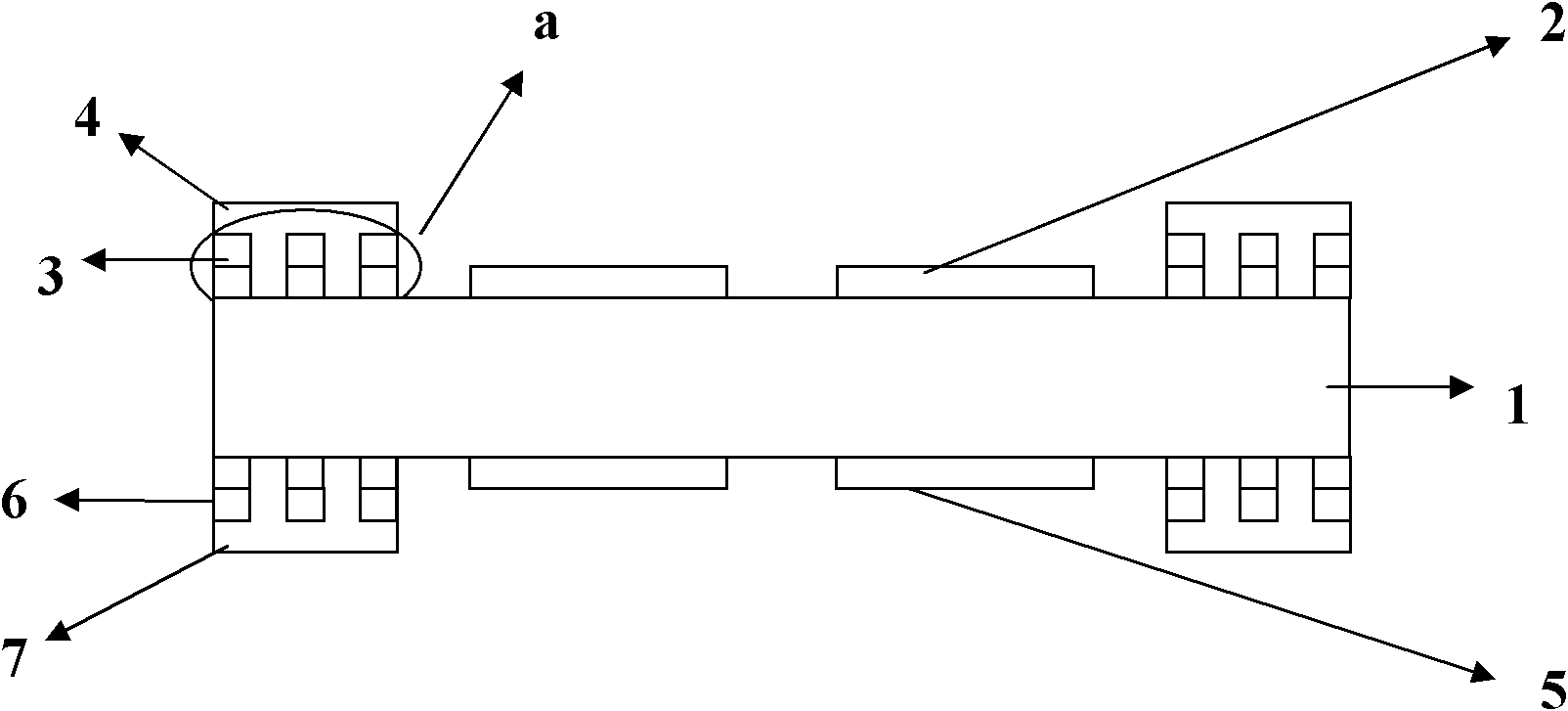
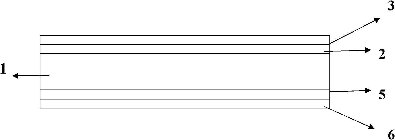
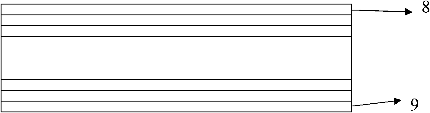
[0034] The roll-type polyethylene terephthalate (PET) film is selected as the base material, and the whole process is operated in a roll-to-roll mode; see Figure 9 . Indium tin oxide (ITO) layer 2 and copper (Cu) layer 3 are successively plated on the upper surface of PET film 1 by vacuum sputtering coating method, and then indium tin oxide (ITO) layer is successively plated on the lower surface by vacuum sputtering coating method. ITO) layer 5 and copper (Cu) layer 6, see figure 2 ; Make photosensitive adhesive layer 8 and layer 9 successively with the mode of screen printing on both sides, refer to image 3 , and then expose, develop, and etch at one time, and make transparent electrode patterns and wiring strengthening patterns at the same time, see Image 6 ; Afterwards, the area where the wiring is strengthened is made of protective adhesive layer 4 and layer 7 by screen printing, see Figure 7 ; The protective glue needs to be able to withstand the immersion of the ...

Embodiment 2

[0036] The difference between this embodiment and Embodiment 1 is that the base material is PET, glass, or PC, or PMMA, or polyolefin, or flexible materials.

Embodiment 3

[0038] The difference between this embodiment and Embodiment 1 is that, in addition to using the method of vacuum sputtering coating to make the transparent conductive layer, it can also be made by vacuum ion coating, vacuum thermal evaporation coating or coating.


PUM

PropertyMeasurementUnit
Thicknessaaaaaaaaaa
Thicknessaaaaaaaaaa

Abstract

The invention relates to a method for manufacturing a sensor structure based on charge transfer. The method comprises the following steps of: manufacturing transparent conductive layers on two surfaces of a base material by a vacuum-sputtering film coating, vacuum ion film coating, vacuum thermal evaporation film coating or coating method; manufacturing metal reinforcement layers on the surfaces of the upper and lower transparent conductive layers by the vacuum-sputtering film coating, vacuum ion film coating or vacuum thermal evaporation film coating method, an electroplating method or a chemical plating method; forming patterns of a first transparent conductive layer, a first lead wire electrode group, a second transparent conductive layer and a second lead wire electrode group on the two surfaces of the base material by a selective erosion method; manufacturing protection layers on the surfaces of the first lead wire electrode group and the second lead wire electrode group by a screen-printing method, a roller transfer-printing method or a photoetching method; and putting a workpiece processed by the process into a selective etching solution to remove the metal reinforcement layers covered on the transparent conductive layers. Compared with the conventional method, the method has the advantages that: the processing procedures are reduced, the process difficulty is lowered, the processing efficiency is improved and the qualification rate is increased greatly, and the manufacturing cost is low.

Description

[0001] technical field [0002] The invention relates to the technical field of electronic display, in particular to a method for fabricating a sensor structure based on charge transfer. Background technique [0003] Touch panels have been widely used in home appliances, communications, electronic information and other product applications, such as handheld computers, various home appliances, and game input interfaces that are currently widely used in commercial use. Both are integrated with a touch panel and a display, allowing users to use their fingers or a stylus to touch and input the actions they want to perform according to the function options on the display screen. [0004] The well-known touch panel mainly arranges a sensing area on the surface of a substrate, and the sensing area is touched by a finger or a stylus to touch an icon or a menu to achieve the purpose of touch. The sensing component is a position sensor based on charge transfer. Most of the materials...

Claims


Application Information

Patent Timeline
IPC IPC(8): G06F3/041
Inventor 张小华潘耀南章晶晶
Owner 南京福莱克斯光电科技有限公司
Why Eureka
Try Eureka