LED (light-emitting diode) packaging structure and manufacturing method thereof

A technology of LED packaging and LED modules, which is applied in the direction of electrical components, electric solid devices, circuits, etc., can solve the problems of low manufacturing efficiency, increased manufacturing cost, and cumbersome process steps, so as to reduce manufacturing cost, improve manufacturing efficiency, and reduce manufacturing costs. cost effect

Inactive Publication Date: 2011-10-12
ENRAYTEK OPTOELECTRONICS
View PDF5 Cites 26 Cited by
  • Summary
  • Abstract
  • Description
  • Claims
  • Application Information

AI Technical Summary

Problems solved by technology

In the current LED chip packaging process, the LED chips must first be diced into individual chip units (die), and then the individual chip units are packaged and connected in series and parallel, which makes the process steps particularly cumbersome. Manufacturing efficiency is lower and manufacturing cost is increased

Method used


Image

  • LED (light-emitting diode) packaging structure and manufacturing method thereof
  • LED (light-emitting diode) packaging structure and manufacturing method thereof
  • LED (light-emitting diode) packaging structure and manufacturing method thereof

Examples


Embodiment Construction

[0055] The LED packaging structure proposed by the present invention and its preparation method will be further described in detail below in conjunction with the accompanying drawings and specific embodiments. Advantages and features of the present invention will be apparent from the following description and claims. It should be noted that all the drawings are in very simplified form and use imprecise ratios, which are only used for the purpose of conveniently and clearly assisting in describing the embodiments of the present invention.
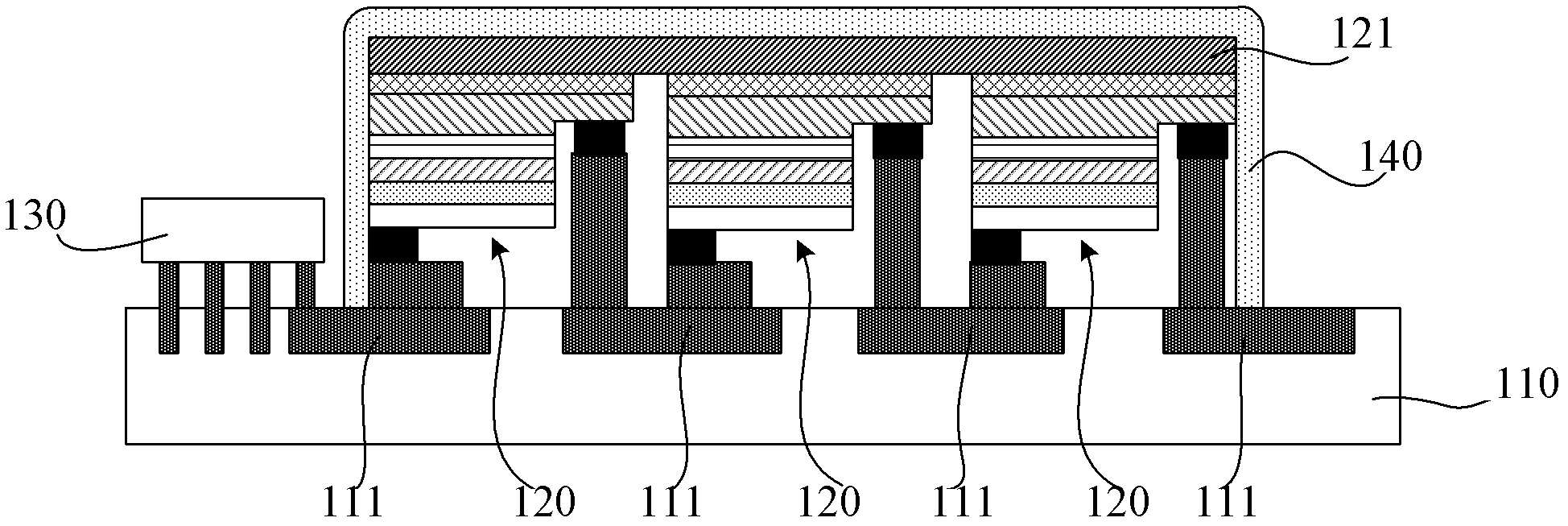
[0056] The core idea of ​​the present invention is to provide an LED package structure, the LED package structure adopts the LED device module structure, so that each LED chip unit does not need to be individually diced, which saves the process and reduces the production cost; and the said The LED packaging structure adopts a flip-chip structure, which is directly flip-chip-fixed on the chip-on-board package bonding pad substrate through met...


PUM


Abstract

The invention discloses an LED (light-emitting diode) packaging structure which is characterized in that an LED device module structure is adopted, thus respective scribing is not carried out on each LED chip, thereby saving processes and reducing manufacturing cost; and an inversion structure is adopted to improve overall performances of LEDs. The invention also discloses a manufacturing method of the LED packaging structure. In the manufacturing method, the LED module, an LED drive circuit and an ESD protection circuit are invertedly fixed on the substrate of a COB (chip on board) packagingbonding tray directly by metal bump spot welding balls, so that the overall performances of the LEDs are improved; and because each LED module comprises a plurality of LED chip units which are connected by the same substrate, the respective scribing is not required to carry out on each LED chip, thus saving the processes and reducing the manufacturing cost.

Description

technical field [0001] The invention relates to the technical field of LED preparation, in particular to an LED packaging structure and a preparation method thereof. Background technique [0002] A light-emitting diode (LED, Light Emitting Diode) is a semiconductor solid-state light-emitting device, which uses a semiconductor PN junction as a light-emitting material, and can directly convert electricity into light. When a forward voltage is applied to both ends of the semiconductor PN junction, the minority carriers injected into the PN junction recombine with the majority carriers, releasing excess energy to cause photon emission, and the direct emission colors are red, orange, yellow, Green, blue, blue, purple light. [0003] In 1998, Lumileds packaged the world's first high-power LED (1W LUXOEN type device), which made LED devices change from the previous application of indicator lights to a new type of solid light source that can replace traditional lighting, triggering...

Claims


Application Information

Patent Timeline
Patent Type & Authority Applications(China)
IPC IPC(8): H01L25/075H01L33/48H01L33/62H01L33/64H01L33/00
CPCH01L2224/14
Inventor 肖德元张汝京程蒙召
Owner ENRAYTEK OPTOELECTRONICS
Why Eureka
Try Eureka