
Signal stability detector and time delay tester

A technology of delay testing and stability, applied in the field of semiconductor technology, can solve the problems of large circuit design complexity and hardware overhead, and achieve the effect of low overhead

Active Publication Date: 2011-10-19
INST OF COMPUTING TECH CHINESE ACAD OF SCI
View PDF4 Cites 10 Cited by
  • Summary
  • Abstract
  • Description
  • Claims
  • Application Information

AI Technical Summary

Problems solved by technology

Therefore, adopting this method will bring great circuit design complexity and hardware overhead

Method used


Image

  • Signal stability detector and time delay tester
  • Signal stability detector and time delay tester
  • Signal stability detector and time delay tester

Examples


Embodiment Construction

[0025] In order to make the object, technical solution and advantages of the present invention clearer, the present invention will be further described in detail below through specific embodiments in conjunction with the accompanying drawings. It should be understood that the specific embodiments described here are only used to explain the present invention, not to limit the present invention.

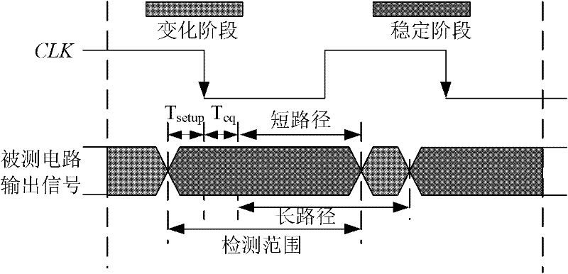
[0026]A complete delay test requires the ability to verify that the propagation delay of any path in the circuit under test exceeds the operating clock period. A path here is a physical path in a combinational circuit, that is, an alternating sequence of leads and gates from the original input of the circuit or the output of the flip-flop to the original output of the circuit or the input of the flip-flop. Since the propagation delays of the rising transition signal and the falling transition signal in the circuit elements are different, each physical path corresponds to two logical pa...


PUM


Abstract

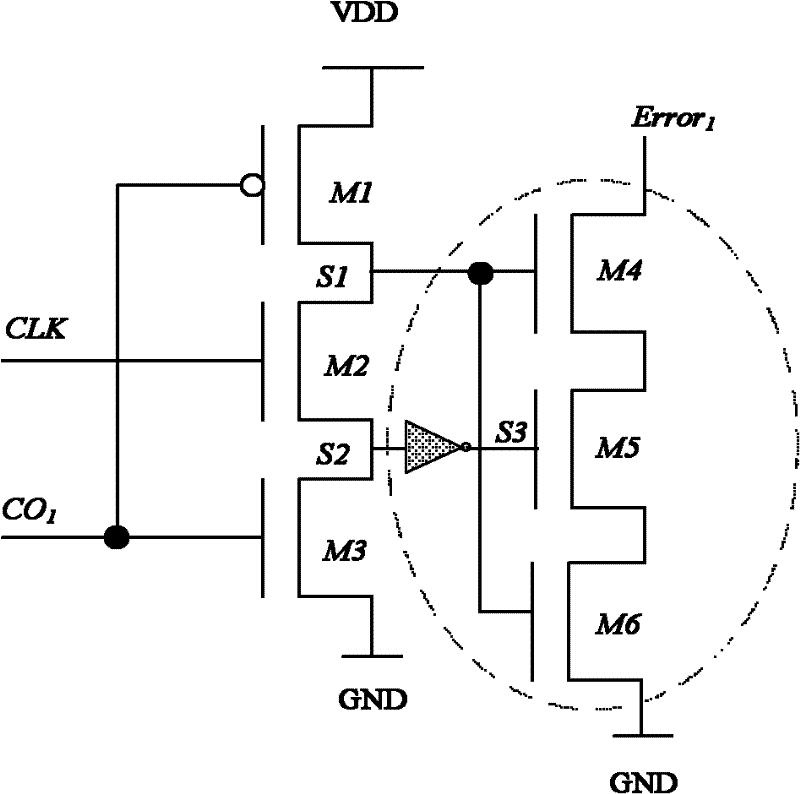
The invention provides a signal stability detector and a time delay tester employing the signal stability detector. Each key combination logic output point of the time delay tester is provided with one corresponding signal stability detector for detecting whether a signal output by each key combination logic output point in the stable period of a combination logic signal rolls over or not; and moreover, the time delay tester is also provided with a global error signal generator for generating a global error signal when any signal stability detector detects that the combination logic signal rolls over in a detection scope so as to indicate the timing out of a circuit. The time delay tester not only can be used for effectively implementing online time delay failure detection, but also applies a partial scan enable signal generator in a scan chain of the circuit. The time delay tester can be used for effectively conducting online time delay failure detection, and can be used for providing effective support for off-line time delay failure detection. Moreover, hardware expenses are lower.

Description

technical field [0001] The invention belongs to the technical field of semiconductor technology, and in particular relates to, in a high-performance chip, effectively detecting the delay fault in the chip to ensure the performance and reliability of the chip. Background technique [0002] With the development of integrated circuit manufacturing technology, the feature size of transistors has been continuously refined. The complexity and level of integration of the entire chip continues to increase. It is becoming more and more obvious that chips contain various defects after they are manufactured, and thus pose serious challenges to the performance and reliability of chips. In addition, under the deep submicron process, it is difficult to accurately control the process parameters in the integrated circuit to the corresponding expected value, but there is a process deviation. As a result, there will be a large time delay deviation in the logic gates and signal propagation p...

Claims


Application Information

Patent Timeline
IPC IPC(8): G01R31/3177
Inventor 裴颂伟李华伟李晓维
Owner INST OF COMPUTING TECH CHINESE ACAD OF SCI
Learn More