Capacitance touch screen and manufacture method thereof

A technology of capacitive touch screen and manufacturing method, which is applied in the direction of electrical digital data processing, ion implantation plating, coating, etc., can solve the problems of uneven and fine wire lines, small touch viewing area of ​​touch screen, and poor resistance uniformity, etc. Achieve the effect of fine and uniform wire lines, good resistance uniformity, and reduce bad air bubbles

Inactive Publication Date: 2011-10-19
TRULY OPTO ELECTRONICS
View PDF5 Cites 2 Cited by
  • Summary
  • Abstract
  • Description
  • Claims
  • Application Information

AI Technical Summary

Problems solved by technology

[0003] 1. The wire made of silk screen printing silver paste has a thickness of about 10 μm, and the air bubbles are caused by large thickness when laminating;
[0004] 2. The wire lines made of silk screen silver paste are not uniform and fine enough, and the resistance uniformity is not good, which affects the performance of the touch screen;
[0005] 3. Due to the limitation of silk screen printing technology, the distance between wires made of silk screen silver paste is generally about 80 μm, which makes the touch viewing area on the touch screen smaller

Method used


Image

  • Capacitance touch screen and manufacture method thereof
  • Capacitance touch screen and manufacture method thereof
  • Capacitance touch screen and manufacture method thereof

Examples


Embodiment Construction

[0022] In order to make the technical solution of the present invention clearer, the present invention will be described in detail below through specific embodiments in conjunction with the accompanying drawings.

[0023] Embodiment of the manufacturing method of the capacitive touch screen:

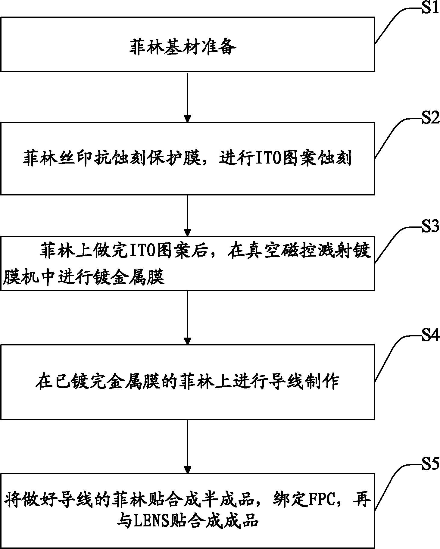
[0024] see image 3 , the manufacture method of capacitive touch screen of the present invention, comprises the steps:

[0025] S1. Film substrate preparation;

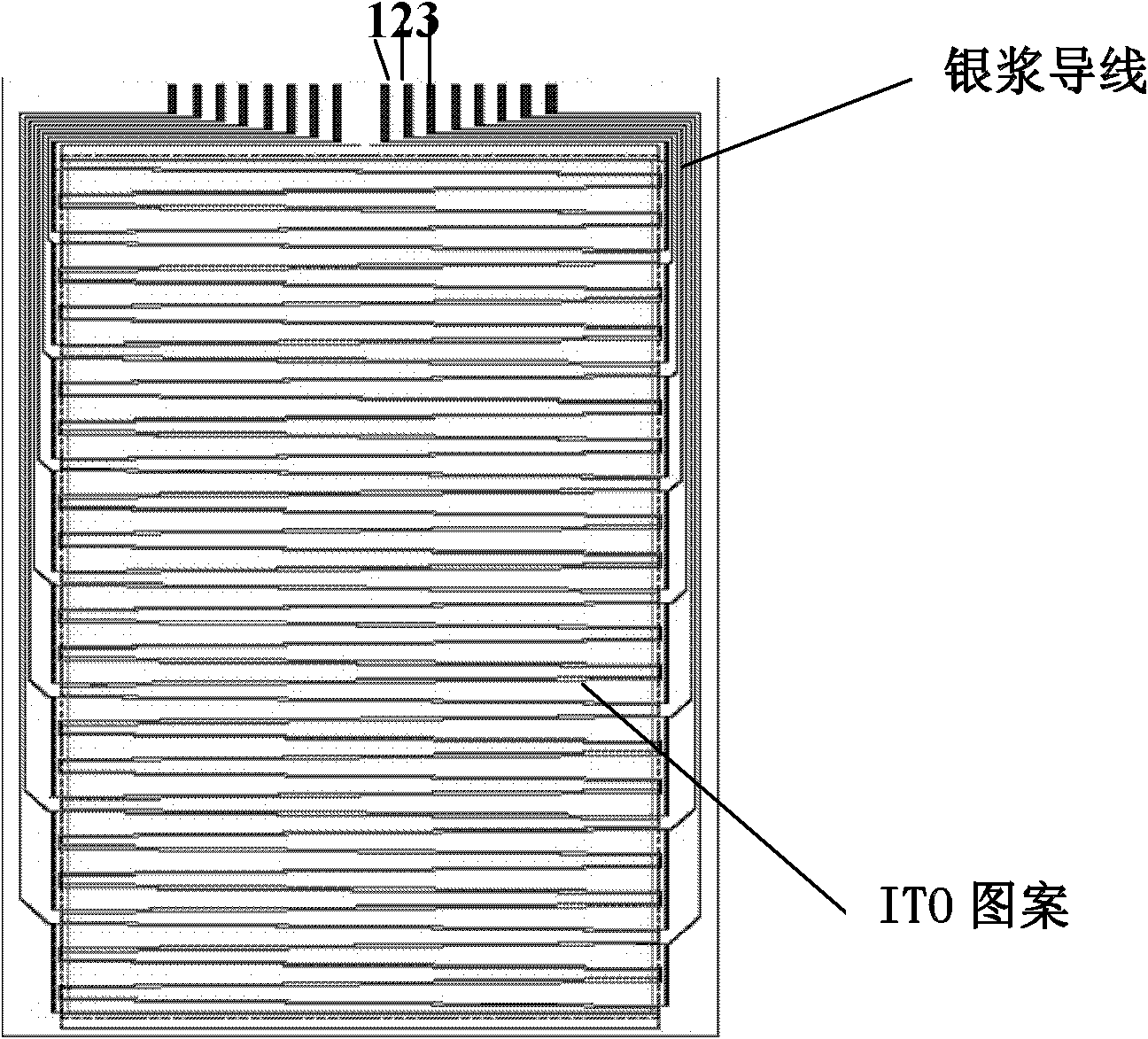
[0026] S2, film silkscreen anti-etching protective film, for ITO pattern etching;

[0027] S3. After the ITO pattern is finished on the film, metallization is performed in a vacuum magnetron sputtering coating machine;

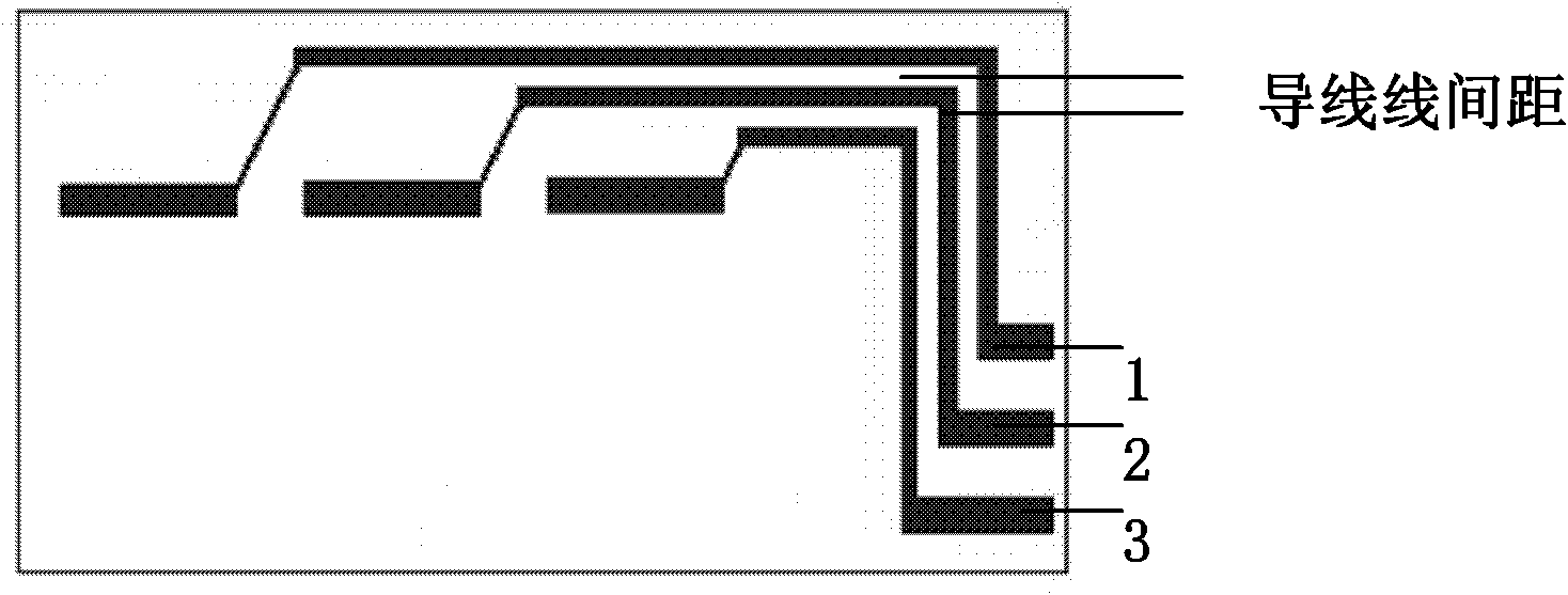
[0028] S4. Carry out wire production on the metal-plated film, that is: form the metal film that has been plated into a wire;

[0029] S5. Paste the wire-finished film into a semi-finished product, bind FPC, and then paste it with LENS to form a finished product.

[0030] Wherein, the film thickness of the ...


PUM

PropertyMeasurementUnit
thicknessaaaaaaaaaa
thicknessaaaaaaaaaa

Abstract

The invention discloses a capacitance touch screen manufacture method, which comprises the steps as follows: after a pattern is etched on a film, a guide wire is manufactured on the surrounding of the pattern by adopting a way of plating a metal film; and then the film is fit with an LENS. The metal guide wire manufactured by adopting the plating way has thickness between 0.3Mu m and 0.6Mu m, which is far smaller than the thickness of 10Mu m of silk-screen silver paste, thus being capable of reducing bad bubbles caused by large thickness during fitting. The guide wire manufactured by the capacitance touch screen manufacture method by adopting the way of plating has fine and uniform lines, which are far higher than that of the silk-screen silver paste, and has good resistance uniformity, thus greatly improving the performances of the touch screen. The distances between the silk-screen silver paste lead wires of the prior art are usually about 80Mu m due to the limitation of a silk-screening technology, however, the distances between the lead wires manufactured by adopting the plating method can be reduced to be 25Mu m, thus having a larger touch visual area on the touch screen with the same size. The invention also discloses a capacitance touch screen.

Description

technical field [0001] The invention relates to a touch screen, in particular to a capacitive touch screen and a manufacturing method thereof. Background technique [0002] Currently, touch screen technology is developing vigorously. Among them, the touch screen technology includes a capacitive touch screen, see figure 1 , figure 2 , the existing capacitive touch screen with film structure is to etch the ITO pattern on the film, and then use the silk screen silver paste method to make the electrode around the ITO pattern. The thickness of the silk screen silver paste is about 10 μm. Bonded into a capacitive touch screen. When the finger touches the surface of the touch screen, a certain amount of charge will be transferred to the human body. In order to restore the charge loss, the charge will be replenished from the four corners of the screen. point position. This method of using silk screen printing silver paste to make wires in the prior art has the following disadv...

Claims


Application Information

Patent Timeline
Patent Type & Authority Applications(China)
IPC IPC(8): G06F3/044C23C14/35C23C14/14
Inventor 蔡汉业朱景河刘亚锋张家添何基强
Owner TRULY OPTO ELECTRONICS
Why Eureka
Try Eureka