Lead frame, semiconductor device using the lead frame, intermediate product thereof, and methods for producing same

A manufacturing method and lead frame technology, which are applied in semiconductor/solid-state device manufacturing, semiconductor devices, semiconductor/solid-state device components, etc., can solve problems such as terminal drop-off, reduced adhesion, and inability to maintain terminal strength, so as to improve bonding Strength and reliability improvement effect

Inactive Publication Date: 2011-10-19
MITSUI HIGH TEC INC
View PDF7 Cites 2 Cited by
  • Summary
  • Abstract
  • Description
  • Claims
  • Application Information

AI Technical Summary

Problems solved by technology

However, due to the demand for higher density and miniaturization of semiconductor devices in recent years, when the thickness of the package or the lead frame becomes thinner or the stand-up height (the distance from the bottom surface of the sealing resin to the surface of the mounting base) increases, the resin The adhesion between the terminals is reduced, so that the strength of the terminals cannot be ensured and the terminals fall off, so there is a problem that the reliability of the semiconductor device is reduced

Method used


Image

  • Lead frame, semiconductor device using the lead frame, intermediate product thereof, and methods for producing same
  • Lead frame, semiconductor device using the lead frame, intermediate product thereof, and methods for producing same
  • Lead frame, semiconductor device using the lead frame, intermediate product thereof, and methods for producing same

Examples


Embodiment Construction

[0063] Embodiments for embodying the present invention will be described with reference to the drawings.

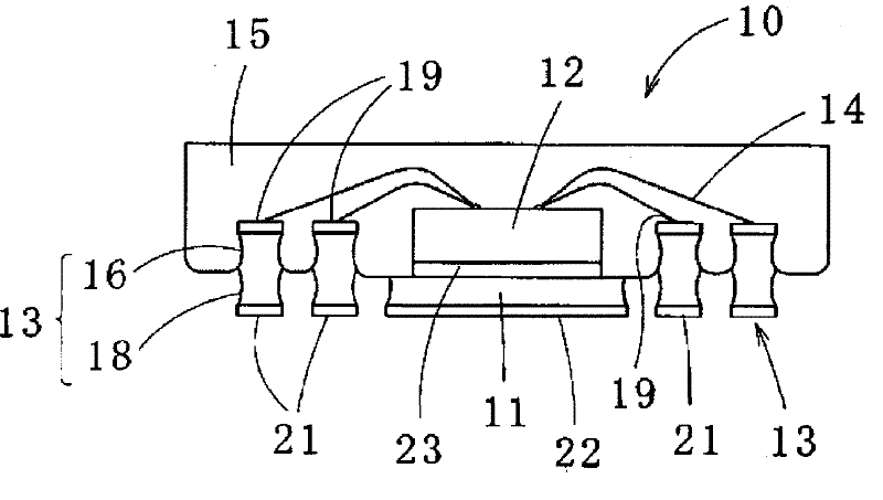
[0064] Such as figure 1 and 2 As shown, the semiconductor device 10 according to the first embodiment of the present invention includes: a semiconductor element 12 placed on a central element mounting portion 11; a plurality of terminals 13 arranged around the semiconductor element 12; and a sealing resin 15 that seals substantially the upper half of the terminal 13, the bonding wire 14, and the semiconductor element 12 with a resin.

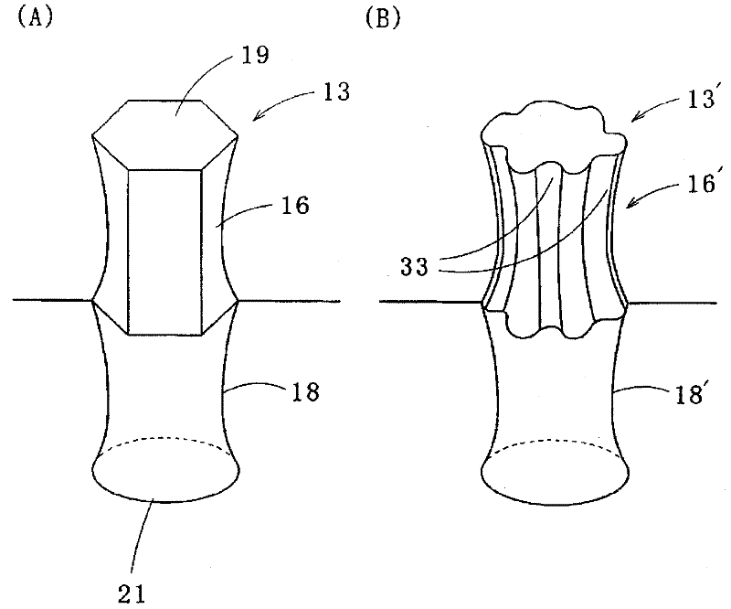
[0065] Here, the shape of the part 16 surrounded by the sealing resin 15 and sealed by the resin of the substantially upper half of the terminal 13 is a hexagonal columnar shape (as an example of a polygonal columnar shape not less than pentagonal), and the substantially lower half of the The exposed portion 18 is cylindrical in shape. In addition, if figure 2 As shown in (A), when the resin-sealed portion 16 is formed by etching, its ...


PUM


Abstract

Disclosed is a lead frame for a semiconductor device (10), which comprises a plurality of terminals (13) having one end portion sealed with a resin. A portion (16) of each terminal (13), which is to be sealed with a resin, is composed of a pentagonal or higher polygonal prism, or an irregular prism having at least one notch or groove which is formed on the peripheral surface and extends in the vertical direction. The portion (16) to be sealed with a resin is formed by etching or pressing, and an exposed portion (18) serving as the lower half of each terminal (13) is formed by etching.

Description

technical field [0001] The present invention relates to a lead frame used in a semiconductor device for improving adhesion with sealing resin, a semiconductor device using the lead frame, an intermediate product of the semiconductor device, the lead frame, the semiconductor device and the intermediate The method by which the product is manufactured. Background technique [0002] Patent Document 1 discloses a method in which a region forming a bonding terminal or the like on the surface of a plate-shaped lead frame material is plated with a noble metal and a resist film is formed, and the thickness is performed from the front side to about one-half of the thickness. Etching (first etching) and mounting semiconductor elements, then performing wire bonding and sealing the lead frame material with resin while leaving the back half of the lead frame material, and etching is selectively performed from the back side (second etch) and cut off adjacent terminals to manufacture a sem...

Claims


Application Information

Patent Timeline
Patent Type & Authority Applications(China)
IPC IPC(8): H01L23/50
CPCH01L21/4832H01L23/3107H01L23/49541H01L23/49548H01L23/49582H01L2224/48091H01L2224/48247H01L2224/48472H01L2224/73265H01L2224/85444H01L2924/01004H01L2924/01057H01L2924/01078H01L2924/01079H01L2224/32257H01L24/48H01L2224/32245H01L2924/181H01L2924/00014H01L2924/00H01L2924/00012H01L2224/45099H01L2224/45015H01L2924/207
Inventor 清水孝司八河博昭
Owner MITSUI HIGH TEC INC
Why Eureka
Try Eureka