Contactless integrated circuit (IC) wafer pad layout design method

A layout design, non-contact technology, applied in the manufacturing of electrical components, electric solid-state devices, semiconductor/solid-state devices, etc., can solve the problems of increasing the amount of gold wire material for chip packaging, increasing product packaging costs, and affecting the packaging yield. The effect of improving the pickup efficiency, improving the pass rate, and simplifying the pickup process

Active Publication Date: 2011-11-09
THE FIRST RES INST OF MIN OF PUBLIC SECURITY +1
View PDF2 Cites 3 Cited by
  • Summary
  • Abstract
  • Description
  • Claims
  • Application Information

AI Technical Summary

Problems solved by technology

According to the current chip designer's Pad layout design method, as long as the non-contact IC chip Pad position is arranged on the side of the chip that is not in the same direction as the Y-axis of the loading table, it will not only increase the amount of chip packaging gold wire material, but also improve the product quality. Packaging cost; and in the process of chip molding and packaging, the inner bonding wire is easily deformed or even broken, which will have a certain impact on the packaging yield, resulting in the problem of unreliable packaging

Method used


Image

  • Contactless integrated circuit (IC) wafer pad layout design method
  • Contactless integrated circuit (IC) wafer pad layout design method
  • Contactless integrated circuit (IC) wafer pad layout design method

Examples


Embodiment Construction

[0016] The specific implementation and installation, configuration and use of a non-contact IC chip Pad layout design method of the present invention will be described below in conjunction with the accompanying drawings.

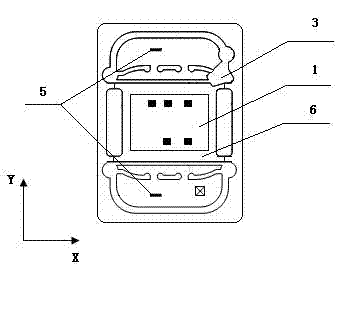
[0017] refer to figure 1 In the figure, the first kind of non-contact IC chip 1 is placed on the first kind of chip carrier table 6 of the first kind of chip carrier frame 3, wherein two antenna solder joints are arranged on the first kind of chip carrier frame 3 5. The chip is connected to the outside (chip carrier tape, coupling antenna) through these two solder joints, so that the IC card can obtain energy from the external system and exchange data with the external system in an electrically coupled manner.

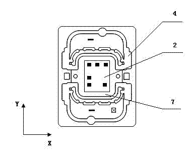
[0018] refer to figure 2 In the figure, the second non-contact IC chip 2 is placed on the second chip carrier platform 7 of the second chip carrier frame 4, wherein the second chip carrier frame 4 is also provided with two antenna soldering Po...


PUM


Abstract

The invention, which relates to the integrated circuit (IC) design technology field, discloses a contactless IC wafer pad layout design method. The invention provides a pad layout design method. A compatibility problem and a reliability packaging problem between pad layout configuration of the current contactless IC wafer and different wafer packaging carrier tape can be solved through arranging two radio frequency function solder joints of the wafer on diagonal positions of the wafer but not the current adjacent angular positions. The invention provides a pad layout design method. After scribing, the wafer can be attached and packaged according to different requirements of a wafer supplier or a wafer packaging trader. By using the method of the invention, a technology communication bridge between the wafer layout design and the wafer packaging are established; the wafer layout design with strong compatibility can be obtained; production efficiency is raised.

Description

technical field [0001] The invention belongs to the technical field of integrated circuit (IC) design, and in particular relates to a non-contact IC chip Pad (pad) layout design method. Background technique [0002] Non-contact IC cards have been widely used for their advantages such as convenient and fast use, low failure rate, high reliability, long life and high environmental tolerance. The non-contact IC chip is the heart of the IC card, and it carries the data of the intended application of the IC card. There are two radio frequency function soldering pads on the chip, and the chip is connected to the outside (chip carrying tape, coupling antenna) through these two soldering pads, so that the IC card can obtain energy from the external system and communicate with the external system by means of electrical coupling. system for data exchange. Therefore, the quality of the connection between the two radio frequency function welding points Pad and the carrier frame direct...

Claims


Application Information

Patent Timeline
Patent Type & Authority Applications(China)
IPC IPC(8): H01L21/50H01L21/60
CPCH01L2224/48247H01L24/06H01L2224/45144H01L2224/05554H01L2924/14
Inventor 侯元香张之津薛艺泽周峥
Owner THE FIRST RES INST OF MIN OF PUBLIC SECURITY
Why Eureka
Try Eureka