

Tube core chip mounting method for ultrathin wafer process
A technology of wafers and dies, which is applied in the field of die bonding in ultra-thin wafer technology, can solve problems such as high production costs and complex processes, and achieve the effects of improving yield rate, increasing mechanical strength, and enhancing mechanical strength
- Summary
- Abstract
- Description
- Claims
- Application Information
AI Technical Summary
Problems solved by technology
Method used
Image

Examples
Embodiment Construction
[0041] According to the claims of the present invention and the content disclosed in the summary of the invention, the technical solution of the present invention is specifically as follows:
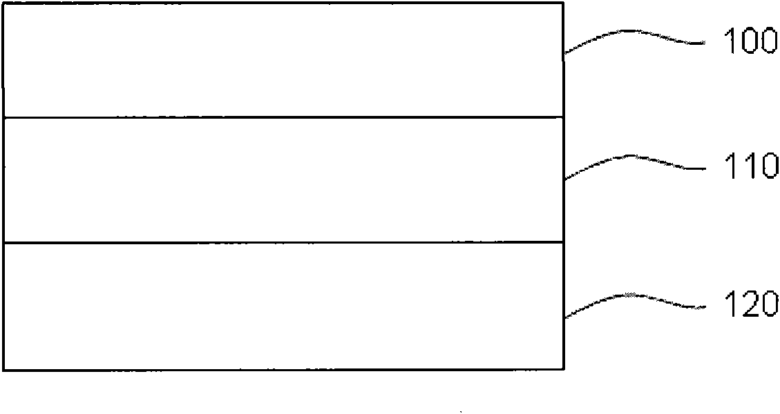
[0042] Such as figure 1 As shown, a kind of single-sided adhesive tape comprises release paper layer 100, thermal release adhesive adhesive layer 110, polyester fiber layer 120, release paper layer 100 is used for protecting thermal release adhesive adhesive layer 110, tear off release adhesive layer 110 during use The paper-shaped layer 100 and the heat-peelable adhesive layer 110 play an adhesive role.
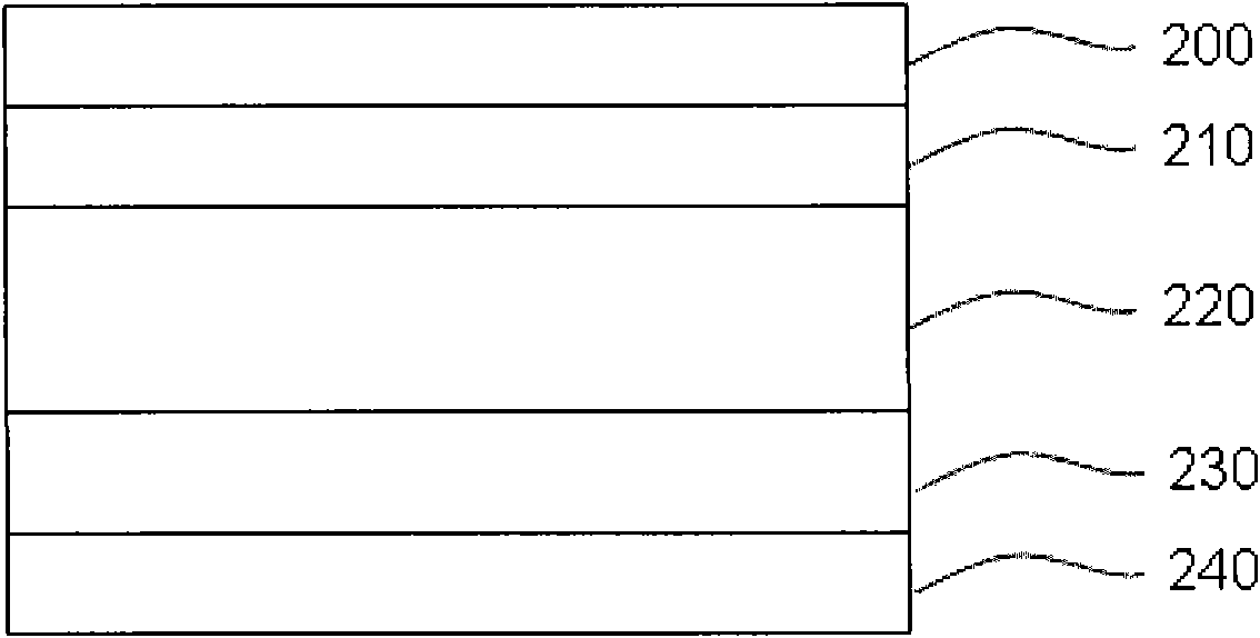
[0043] Such as figure 2 As shown, relative to the above-mentioned single-sided adhesive tape, the double-sided heat release tape comprises a release paper layer 200, another release paper layer 240, a heat release adhesive layer 210, a polyester fiber layer 220, a pressure sensitive adhesive layer 230. The release paper layer 200 and another release paper layer 240 are respectively...
PUM
 Abstract
Description
Claims
Application Information