Two-dimensional micro-electromechanical system (MEMS) tilting mirror with freely changeable deflection axis

A technology of tilting mirrors and deflection axes, which is applied in optical components, optics, instruments, etc., can solve the problems of increasing the production cost of two-dimensional MEMS tilting mirrors and reducing the quality of optical path modulation, so as to improve the conversion efficiency and quality of optical paths, and achieve efficient and reliable optical paths The effect of the conversion

Inactive Publication Date: 2013-07-10
INST OF OPTICS & ELECTRONICS - CHINESE ACAD OF SCI
View PDF5 Cites 0 Cited by
  • Summary
  • Abstract
  • Description
  • Claims
  • Application Information

AI Technical Summary

Problems solved by technology

However, the deflection axis of the mirror is fixed and cannot be moved. For specific requirements, it is necessary to design a specific mirror structure so that the two deflection axes of the mirror intersect at a specific angle, so that the optical path that needs to be converted is just conveniently modulated by the mirror that rotates around this axis. , which increases the production cost of the two-dimensional MEMS tilting mirror, and due to the existence of design and processing errors, the angle between the two deflection axes of the processed two-dimensional MEMS tilting mirror is always different from the design requirements, such as the design in Document 1 The included angle between the two deflection axes is 145°, but the actual angle is 145.37°, resulting in a decline in the modulation quality of the optical path by the tilting mirror

Method used


Image

  • Two-dimensional micro-electromechanical system (MEMS) tilting mirror with freely changeable deflection axis
  • Two-dimensional micro-electromechanical system (MEMS) tilting mirror with freely changeable deflection axis
  • Two-dimensional micro-electromechanical system (MEMS) tilting mirror with freely changeable deflection axis

Examples


Embodiment Construction

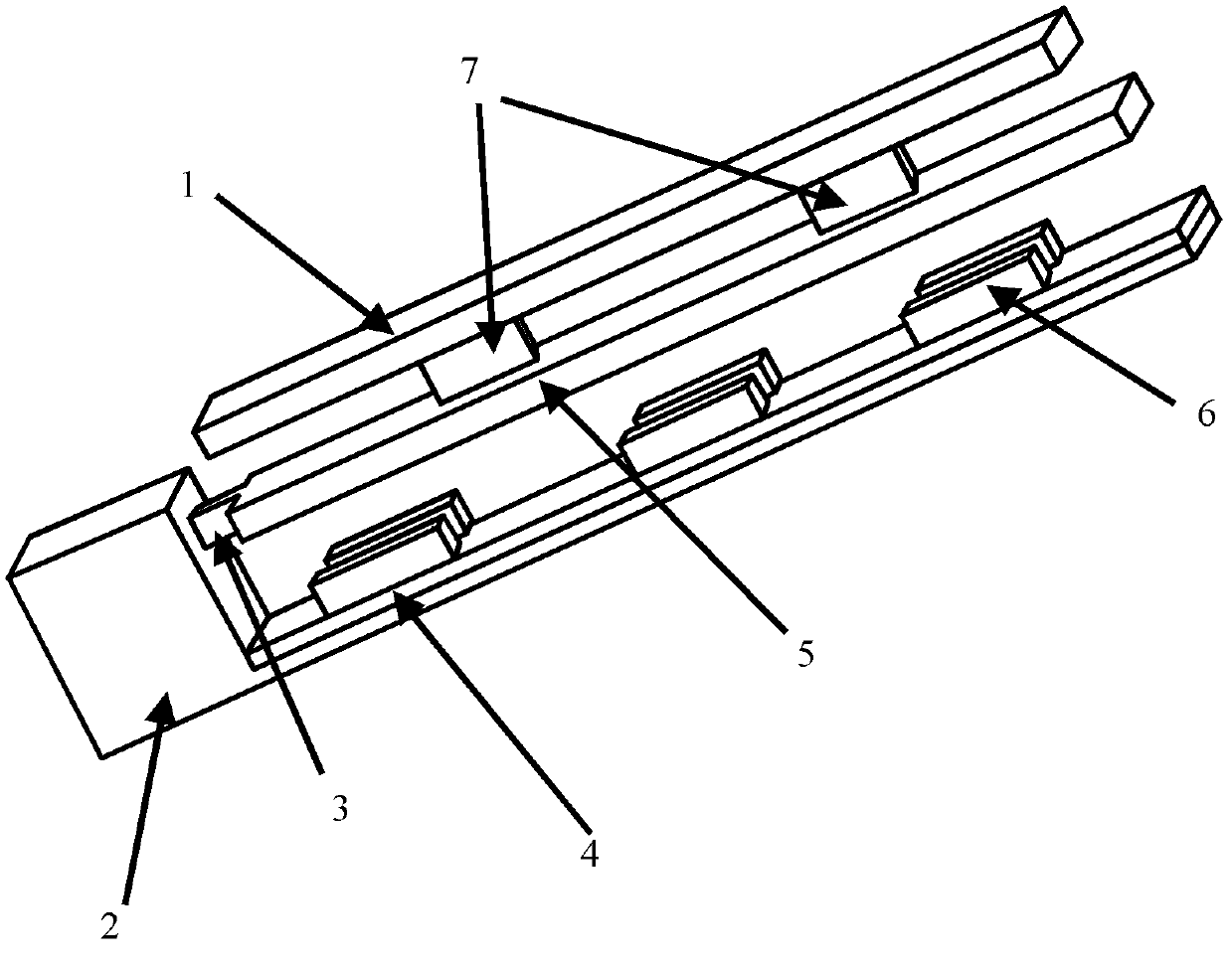
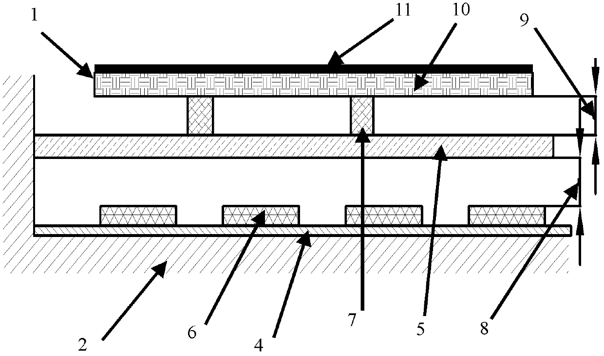
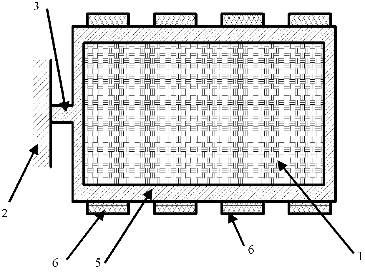
[0053] In order to solve the deficiencies in the optical path conversion of the two-dimensional MEMS tilting mirror with fixed deflection axis in the background technology, and improve the optical path conversion efficiency and quality of the two-dimensional MEMS tilting mirror, the present invention provides a two-dimensional MEMS tilting mirror whose deflection axis can be freely transformed mirror.

[0054] see figure 1 , 2 , 3, 4, 5 and Figure 6, which are respectively the structural schematic diagram of the two-dimensional MEMS tilting mirror whose deflection axis can be freely transformed in the present invention, the cross-sectional schematic diagram of the two-dimensional MEMS tilting mirror whose deflection axis can be freely transformed, the top view of the two-dimensional MEMS tilting mirror whose deflection axis can be freely transformed, and the deflection axis The arrangement diagram of the upper electrode 5 and the lower electrode block 6 of the two-dimension...


PUM


Abstract

The invention discloses a two-dimensional micro-electromechanical system (MEMS) tilting mirror with a freely changeable deflection axis. An upper electrode is fixed on a substrate in a single side asymmetrical mode, and the deflection axis of the two-dimensional MEMS tilting mirror is freely changed by applying the same voltage value onto a lower electrode block of the tilting mirror in differentarrangement modes or applying different voltage values onto the lower electrode block of the tilting mirror in the same arrangement mode or comprehensively using the two schemes. The tilting mirror has high flexibility, the light path conversion efficiency and quality of the tilting mirror are effectively improved, the using cost is reduced, and contribution to further application of the tilting mirror in the fields of optical communication, projection display, optical imaging, laser confocal microscope and the like is facilitated.

Description

technical field [0001] The invention belongs to the production field of MEMS (Micro-electromechanical Systems) tilting mirrors, and relates to the design and manufacture of MEMS tilting mirrors used in the fields of optical communication, projection display, optical imaging, laser confocal microscopy, etc., and specifically relates to a deflection axis that can be freely transformed 2D MEMS tilting mirror. Background technique [0002] Optical tilting mirrors have important application value in optical communication, projection display, optical imaging and laser confocal microscopy system. In addition to the low cost and easy mass production common to MEMS devices, the MEMS tilting mirror also has the advantages of fast dynamic response and low power consumption. The two-dimensional MEMS tilting mirror can realize two-dimensional optical path conversion on one device, with small space occupation and high work efficiency. [0003] The deflection axes of traditional two-dime...

Claims


Application Information

Patent Timeline
Patent Type & Authority Patents(China)
IPC IPC(8): G02B26/08
Inventor 庄须叶姚军
Owner INST OF OPTICS & ELECTRONICS - CHINESE ACAD OF SCI
Why Eureka
Try Eureka