Method for analyzing and checking local pattern density of chip

A technology of pattern density and inspection method, applied in the field of pattern density analysis and inspection, can solve problems such as manual screening, false alarms, and inability to achieve inspection results, and achieve the effect of avoiding false alarms and improving inspection capabilities.

Active Publication Date: 2013-02-13
SHANGHAI HUAHONG GRACE SEMICON MFG CORP
View PDF4 Cites 2 Cited by
  • Summary
  • Abstract
  • Description
  • Claims
  • Application Information

AI Technical Summary

Problems solved by technology

[0005] However, if the local area is simply reduced, many false alarms will be caused, and manual screening is necessary, so that the inspection effect cannot be achieved

Method used


Image

  • Method for analyzing and checking local pattern density of chip
  • Method for analyzing and checking local pattern density of chip
  • Method for analyzing and checking local pattern density of chip

Examples


Embodiment Construction

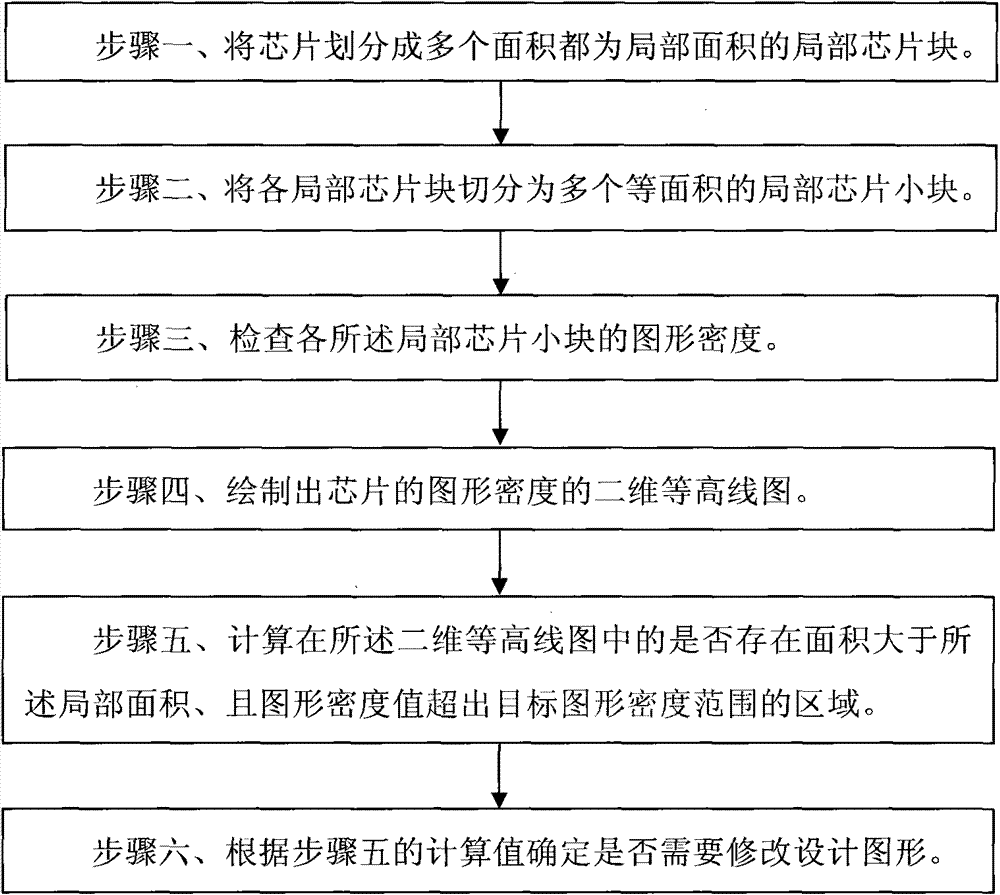
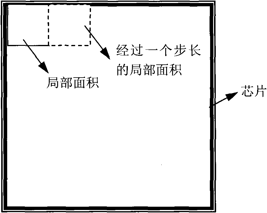
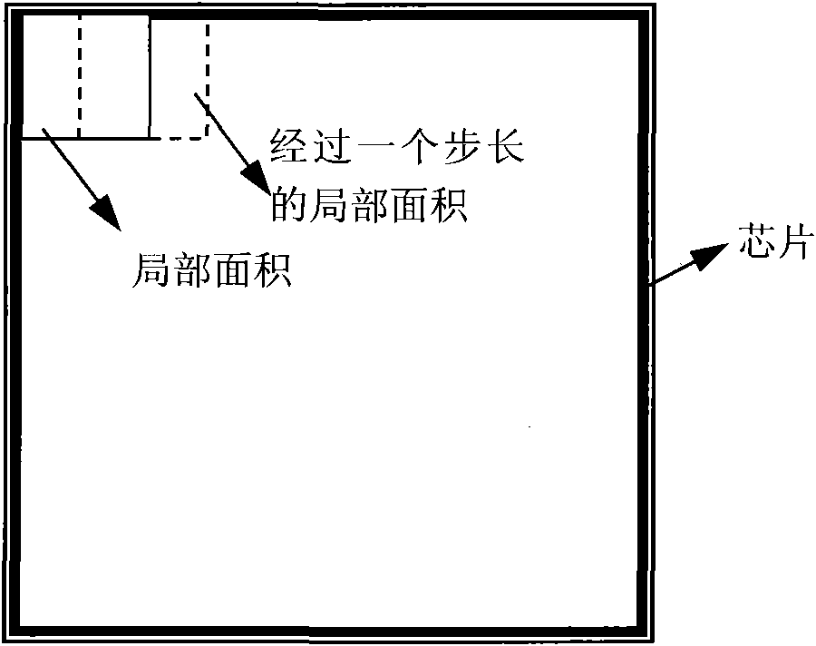
[0023] An embodiment of the present invention is listed below and the advantages of the present invention are described in combination with the prior art. For a chip that requires measurement, the chip is divided into a plurality of rectangular local chip blocks according to the size of a local area, and it is assumed that the target pattern density range of the local chip blocks with a local area size of this type of chip is <= 30%. In the embodiment of the present invention, the chip is divided into 12 identical local chip blocks in 3 equal parts in the X direction and 4 equal parts in the Y direction according to the size of the local area.

[0024] One, adopt the local pattern density inspection method of prior art chip to check a pair of described chip, obtain the data as described in table 1, can find out that the pattern density of 12 each described local chip block has been checked altogether, and all The pattern densities of the local chip blocks are all less than 30...


PUM


Abstract

The invention discloses a method for analyzing and checking the local pattern density of a chip. The method comprises the following steps of: 1, defining the size of a local area according to chemical mechanical polarization (CMP) and the requirement of an etching process for macro loading, and dividing the chip into a plurality of local chip blocks of which the area is local area; 2, cutting each local chip block into a plurality of small equal-area local chip blocks; 3, checking the pattern density of each small local chip block; 4, drawing a two-dimensional contour chart of the pattern density of the chip; 5, calculating whether a region of which the area is larger than the local area and a pattern density value is beyond the density range of a target pattern exits in the two-dimensional contour chart; and 6, judging whether the design pattern is required to be changed according to a calculation value in the step 5. By the method, the checking capacity of the pattern density is enhanced without increase of false warning cases during checking of the pattern density.

Description

technical field [0001] The invention relates to the field of semiconductor integrated circuit manufacturing, in particular to a method for analyzing and checking pattern density of a chip. Background technique [0002] With the continuous improvement of integrated circuit process technology, especially after the 0.13 micron process, the line width of the silicon process is already smaller than the wavelength length of exposure, making process stability more and more difficult. In the early stage of design, the derivative effect of the process is considered, resulting in a lot of design rule checks (DRC, Design Rule Check). Design rule checking includes many aspects. Among them, the overall and local pattern density (Pattern Density) has a great influence on chemical mechanical polishing (CMP, Chemical Mechanical Polarization) and etching macro loading (Macro Loading). In the prior art, there are cases where the pattern density of the active area (AA, Active Area) violates ...

Claims


Application Information

Patent Timeline
Patent Type & Authority Patents(China)
IPC IPC(8): H01L21/00H01L21/66
Inventor 陈福成
Owner SHANGHAI HUAHONG GRACE SEMICON MFG CORP
Why Eureka
Try Eureka