Flexible substrate package-based shielding structure and manufacturing process thereof

A flexible substrate and shielding structure technology, applied in the fields of magnetic field/electric field shielding, semiconductor/solid-state device manufacturing, semiconductor/solid-state device components, etc. Conducive to miniaturization, easy heat dissipation, good reliability and mechanical properties

Inactive Publication Date: 2011-11-23
INST OF MICROELECTRONICS CHINESE ACAD OF SCI
View PDF10 Cites 27 Cited by
  • Summary
  • Abstract
  • Description
  • Claims
  • Application Information

AI Technical Summary

Problems solved by technology

This type of structure is only for substrate shielding, that is, it can only shield the internal circuit of the flexible substrate, and cannot solve the EMI problem of components in the package
And this type of patent protects a specific shielding flexible substrate structure, which is not unique, that is, a flexible substrate with shielding performance can also be realized by using conventional methods and other special structures

Method used


Image

  • Flexible substrate package-based shielding structure and manufacturing process thereof
  • Flexible substrate package-based shielding structure and manufacturing process thereof
  • Flexible substrate package-based shielding structure and manufacturing process thereof

Examples


no. 1 example

[0043] figure 1 is a cross-sectional view of a single-layer shielding structure based on a flexible substrate package according to the first embodiment of the present invention. Such as figure 1 As shown, the bare chip 103 is bonded on the flexible substrate 101 in a Flip-chip manner, and the underfill glue 107 is used to protect the Flip-Chip bumps 104 . The shielding layer 102 is located on the flexible substrate 101 and is connected to the substrate ground / power circuit or directly connected to the ground / power BGA solder ball 105 through conductive vias. The material of the shielding layer is a metal film such as copper or coated with shielding glue. The shielding glue includes common shielding glue and new colloids containing high magnetic permeability and high conductivity micro-particles such as iron, cobalt, nickel or corresponding alloys. A potting compound 106 such as plastic compound is filled between the folded flexible substrate 101 and the bare chip 103 to fix th...

no. 2 example

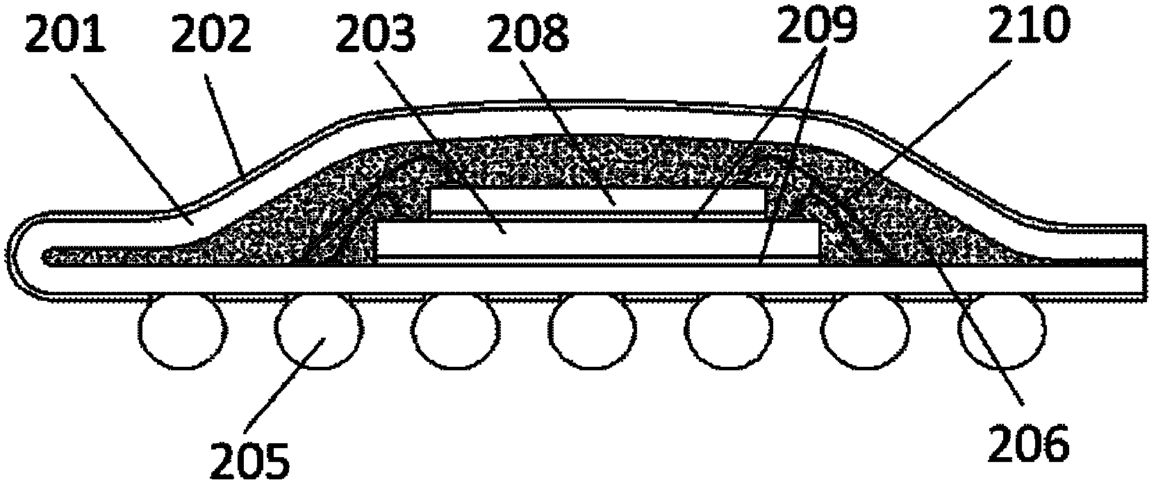
[0045] figure 2 is a cross-sectional view of a single-layer shielding structure based on flexible substrate packaging according to the second embodiment of the present invention. Such as figure 2 As shown, the bare chip 203 is fixed on the chip 208 through the adhesive 209, the bare chip 208 is fixed on the flexible substrate 201 through the adhesive, the shielding layer 202 is located on the flexible substrate 201, and is grounded / connected to the substrate through the conductive via hole The power circuit is connected or directly connected to the ground / power BGA ball 205 . The material of the shielding layer is a metal film such as copper or coated with shielding glue. The shielding glue includes common shielding glue and new colloids containing high magnetic permeability and high conductivity micro-particles such as iron, cobalt, nickel or corresponding alloys. A potting compound 206 such as plastic compound is filled between the folded flexible substrate 201 and the b...

no. 3 example

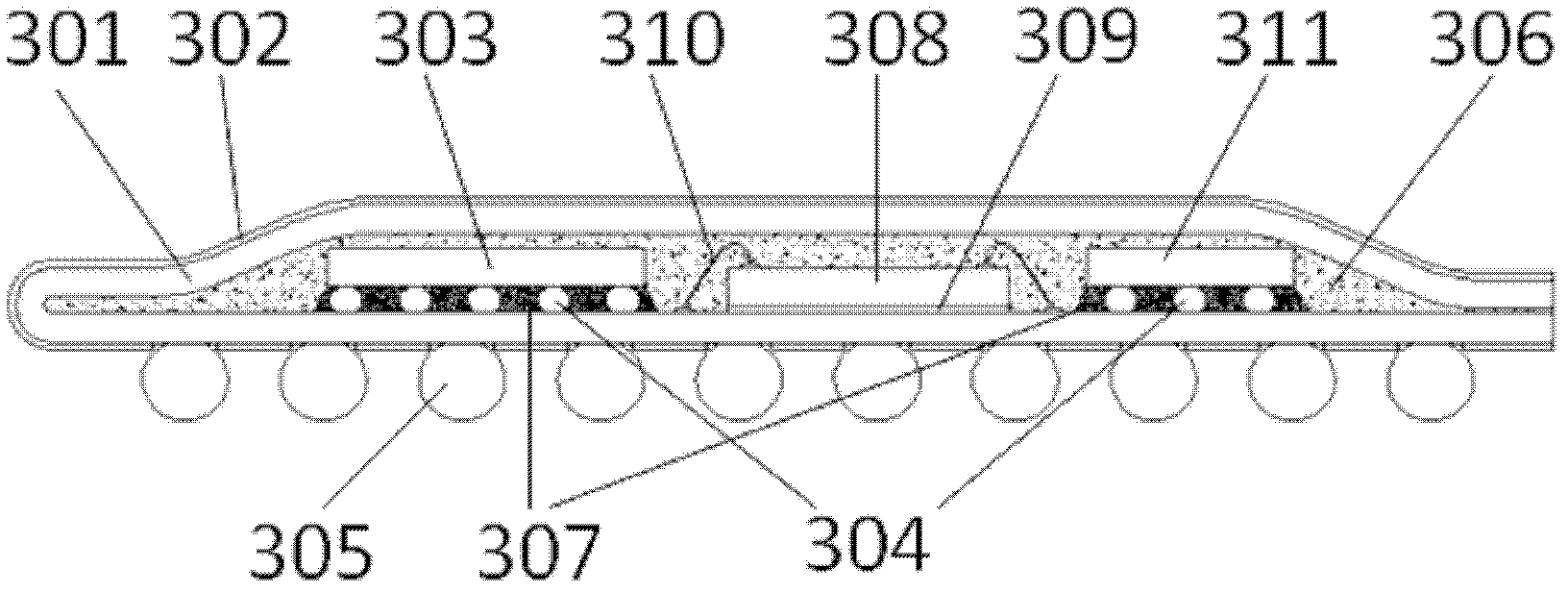
[0047] image 3 is a cross-sectional view of a single-layer shielding structure based on flexible substrate packaging according to the third embodiment of the present invention. Such as image 3 As shown, the bare chips 301 and 311 are bonded on the flexible substrate 301 in a Flip-chip manner, the underfill glue 307 is used to protect the Flip-Chip bumps 304, and the bare chip 308 is fixed on the flexible substrate 301 by an adhesive 309. The shielding layer 302 is located on the flexible substrate 301 and connected to the substrate ground / power circuit or directly connected to the ground / power BGA solder ball 305 through conductive vias. The material of the shielding layer is a metal film such as copper or coated with shielding glue. The shielding glue includes common shielding glue and new colloids containing high magnetic permeability and high conductivity micro-particles such as iron, cobalt, nickel or corresponding alloys. A potting compound 306 such as plastic compoun...


PUM


Abstract

The invention relates to a flexible substrate package-based shielding structure and a manufacturing process thereof. The shielding structure comprises a flexible substrate which is coated on a component, wherein a potting adhesive is filled between the flexible substrate and the component; at least one shielding layer is coated on the flexible substrate; the shielding layer is grounded or connected with a power supply; a plurality of packaging pins are arranged on an outer surface of the flexible substrate with the shielding layer; the packaging pins are electrically connected with the flexible substrate; and the flexible substrate is interconnected with a printed circuit board through the packaging pins. For the flexible substrate package-based shielding structure, the manufacturing process is basically mature, the packaging weight is light, and the sensitivity of a miniature packaging system can be effectively improved.

Description

technical field [0001] The invention relates to a shielding structure based on flexible substrate packaging and a manufacturing process thereof, in particular to a shielding structure for single-chip packaging and a system-in-package (SiP) and a manufacturing process thereof, belonging to the technical field of microelectronic packaging. Background technique [0002] With the rise of communication electronics, the demand for miniaturized and high-sensitivity modules or systems is getting higher and higher, and the requirements for signal quality are becoming more and more stringent. The sensitivity of general communication systems is -100dBm, and the sensitivity of GPS (Global Positioning System) is even lower than -148dBm. The sensitivity requirements of some transceiver modules are also very high. Electromagnetic compatibility (EMI) has become a very important part of the system miniaturization package. The problem. EMI problems mainly include the interference of the ext...

Claims


Application Information

Patent Timeline
Patent Type & Authority Applications(China)
IPC IPC(8): H01L23/538H01L23/552H01L21/48
CPCH01L24/32H01L2224/48227H01L2225/06568H01L2924/15311H01L2225/06537H01L25/0655H01L2924/3025H01L2224/73204H01L2225/06558H01L25/50H01L24/16H01L2924/01322H01L2225/06517H01L2224/32225H01L23/4985H01L24/48H01L2224/73265H01L2225/0651H05K9/0024H01L2224/16227H01L23/552H01L2224/16225H01L23/3128H01L2224/32145H01L25/0657H01L24/73H01L2924/00014H01L2924/181H01L2924/00H01L2924/00012H01L2224/0401H01L2224/45099
Inventor 李君万里兮曹立强陶文君
Owner INST OF MICROELECTRONICS CHINESE ACAD OF SCI
Why Eureka
Try Eureka