Calibration device for optical system wave aberration and calibration method for test error of the device

A technology of an optical system and a calibration device, applied in the field of optical measurement, can solve the problems of test error, inability to evaluate the test error detection accuracy requirements, etc.

Inactive Publication Date: 2011-11-30
CHANGCHUN INST OF OPTICS FINE MECHANICS & PHYSICS CHINESE ACAD OF SCI
View PDF8 Cites 29 Cited by
  • Summary
  • Abstract
  • Description
  • Claims
  • Application Information

AI Technical Summary

Problems solved by technology

[0012] The present invention provides an optical system wave aberration calibration device and an Calibration method of the test error of the device

Method used


Image

  • Calibration device for optical system wave aberration and calibration method for test error of the device
  • Calibration device for optical system wave aberration and calibration method for test error of the device
  • Calibration device for optical system wave aberration and calibration method for test error of the device

Examples


specific Embodiment approach 1

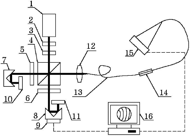
[0023] Specific implementation mode 1. Combination figure 1 Describe the present embodiment, optical system wave aberration calibrating device, this device comprises spectroscopic system, coupling lens 12, reference optical fiber 13, motorized polarization controller 14, photodetector 15, computer 16; It is characterized in that, described spectroscopic system comprises Laser 1, neutral density filter 2, half-wave plate 3, polarization beam splitter prism 4, first quarter-wave plate 5, second quarter-wave plate 6, first corner cube prism 7 , the second corner cube prism 8, the first plane reflector 10 and the second plane reflector 11; the light beam emitted by the laser 1 passes through the neutral density filter 2, the half-wave plate 3 and the polarization beam splitter prism 4 After that, be divided into two beams of orthogonal linearly polarized light, the first beam of linearly polarized light passes through the first quarter-wave plate 5 and the first corner cube prism ...

specific Embodiment approach 2

[0027] Specific embodiment two, the calibration method of the test error of the optical system wave aberration calibration device, the method is completed by the following steps:

[0028] Step 1. Two beams of orthogonal linearly polarized light with a common optical path emitted by the beam splitting system are emitted by the polarization beam splitter prism 4 and then coupled into the reference fiber through the coupling lens 12. The two spherical waves diffracted by the reference fiber 13 interfere to obtain an interference pattern ;

[0029] Step 2. The interferogram obtained in step 1 is collected by the photodetector 15 and then sent to the computer 16, and the piezoelectric ceramic 9 is used for phase shifting. The photoelectric detector 15 collects multiple interferograms; using thirteen steps of phase shifting Algorithms for data processing and analysis to obtain test errors;

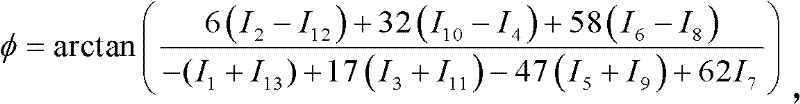
[0030] The thirteen-step phase-shifting algorithm is:

[0031] φ = ...


PUM


Abstract

An optical system wave aberration calibration apparatus and a calibration method of using the apparatus to test an error relate to the optical measurement technology field. The current optical system can not evaluate whether the test error satisfies a detection precision requirement before detecting an optical element and the current optical system can not select an appropriate phase shifting algorithm to process collected data. The above problems can be solved by using the invention. The method comprises the following steps: a light splitting system emits two beams of common-optical-path orthogonal-line polarized lights and after being emitted by a polarization splitting prism, the polarized lights are coupled to a reference fiber through a coupling lens; two spherical waves diffracted by the reference fiber perform interference and an interferogram can be acquired; a photoelectric detector is used to collect the interferogram and to transmit to a computer; piezoelectric ceramics areused to carry out phase shifting and the photoelectric detector collects the interferogram several times; a thirteen step phase shifting algorithm is used to carry out data processing analysis so as to obtain the test error. By using the invention, ultrahigh precision testing of the optical system wave aberration can be realized.

Description

technical field [0001] The invention relates to the technical field of optical measurement, in particular to a calibration device for wave aberration of an optical system and a calibration method for testing errors of the device. Background technique [0002] Extreme ultraviolet lithography is a next-generation lithography technology based on traditional optical lithography, which inherits the development achievements of current optical lithography to the greatest extent. The working wavelength of extreme ultraviolet lithography is the extreme ultraviolet band of 13-14nm. There are major differences between traditional optical lithography and detection technology. As one of the core unit systems of the lithography machine, in order to achieve the requirements of lithography resolution and critical dimension control, the RMS wave aberration of the optical system should be less than λ / 20. Such a high-precision optical system requires a higher-precision detection device. At p...

Claims


Application Information

Patent Timeline
Patent Type & Authority Applications(China)
IPC IPC(8): G01M11/02
Inventor 金春水王丽萍张宇
Owner CHANGCHUN INST OF OPTICS FINE MECHANICS & PHYSICS CHINESE ACAD OF SCI
Why Eureka
Try Eureka