Wafer Formation Method

A wafer and wafer boat technology, applied in the field of wafer formation, can solve problems such as poor wafer quality and affecting the performance of semiconductor devices, and achieve the effects of improving quality, increasing gaps, and consistent stress

Active Publication Date: 2011-11-30
SHANGHAI HUAHONG GRACE SEMICON MFG CORP
View PDF4 Cites 3 Cited by
  • Summary
  • Abstract
  • Description
  • Claims
  • Application Information

AI Technical Summary

Problems solved by technology

[0007] However, the quality of the wafers annealed in the prior art is poor, so that other functional layers, such as photoresist layers, will be dislocated later on the wafers, which will affect the performance of the formed semiconductor devices

Method used


Image

  • Wafer Formation Method
  • Wafer Formation Method
  • Wafer Formation Method

Examples


Embodiment Construction

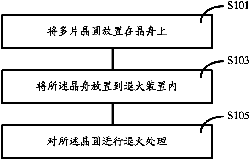
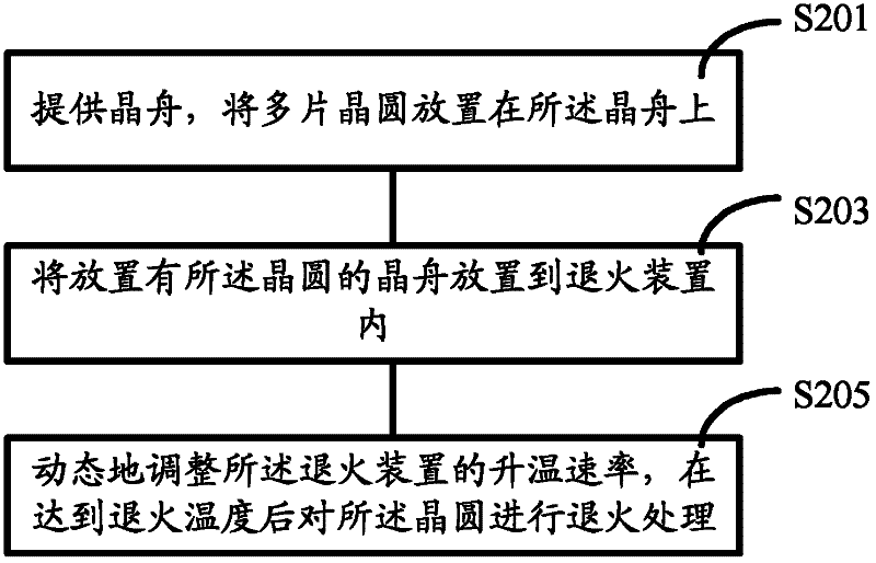
[0032] As mentioned in the background art, the wafer forming method in the prior art has poor quality of the formed wafer, resulting in poor performance of the semiconductor devices formed on the wafer.

[0033] The inventors of the embodiments of the present invention found after research that the poor quality of wafers formed by the prior art is mainly reflected in two aspects: macroscopically and microscopically: macroscopically, when the wafer is annealed, the temperature of the wafer edge rises more Fast, the temperature at the edge of the wafer is higher than the temperature at the center of the wafer, causing the wafer at the edge to soften, so under the action of gravity, the wafer at the center slides down, causing the wafer to deform, and the wafer’s The quality deteriorates; microscopically, when the wafer is annealed, the temperature rise rate at the edge of the wafer is higher than the temperature rise rate at the center of the wafer. Due to the uneven temperature ...


PUM


Abstract

An embodiment of the present invention provides a method for forming a wafer, comprising: providing a wafer boat, placing a plurality of wafers on the wafer boat; placing the wafer boat on which the wafers are placed in an annealing device; The heating rate of the annealing device is dynamically adjusted, and the wafer is annealed after reaching the annealing temperature. By adopting the method of the embodiment of the present invention, the quality of the formed wafer is good, it is not easy to be deformed, and the crystal lattice inside the wafer is not easy to slip or dislocate.

Description

technical field [0001] The invention relates to the technical field of semiconductor manufacturing, in particular to a method for forming a wafer. Background technique [0002] With the advancement of science and technology, semiconductor electronic products have been applied to various fields of social life, and these semiconductor electronic products are all made on wafers. It can be seen that wafers play a very significant role in today's life. [0003] During the wafer formation process, annealing is an indispensable step to eliminate lattice defects and internal stress inside the wafer. Please refer to figure 1 , a method for forming a wafer of the prior art, comprising: [0004] Step S101, placing multiple wafers on the wafer boat; [0005] Step S103, placing the wafer boat into an annealing device; [0006] Step S105, annealing the wafer. [0007] However, the quality of the wafers annealed in the prior art is poor, so that other functional layers, such as photor...

Claims


Application Information

Patent Timeline
Patent Type & Authority Applications(China)
IPC IPC(8): H01L21/324H01L21/673
Inventor 王硕许忠义
Owner SHANGHAI HUAHONG GRACE SEMICON MFG CORP
Why Eureka
Try Eureka