

In-situ melting and reflow process and system for forming flip-chip interconnects
A melting temperature and displacement technology, applied in electrical components, circuits, manufacturing tools, etc., to solve problems such as increased electrical short circuits, poor reliability and quality of semiconductor packaging, and short circuits
- Summary
- Abstract
- Description
- Claims
- Application Information
AI Technical Summary
Problems solved by technology
Method used
Image

Examples
Embodiment Construction
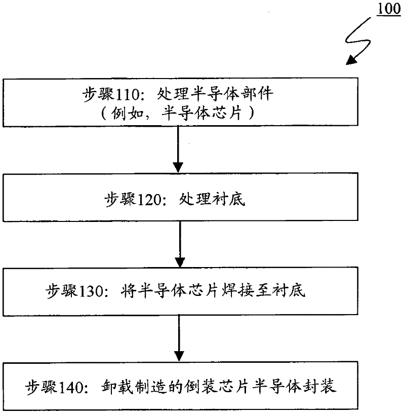
[0034] The current method of manufacturing flip-chip semiconductor packages is to heat the assembly of semiconductor chip and device carrier (eg, substrate) Solder bumps formed on pads or pillars of the semiconductor chip are placed on contact pads formed on the device carrier. This heating process is generally time-consuming, thereby adversely affecting the manufacturing or production efficiency and throughput of flip-chip semiconductor packages. Existing methods also generally involve the use of considerable force to bring the pads of the semiconductor chip into abutment with the contact pads of the device carrier, thereby producing reliable solder joints. Consequently, use of considerable force during its heating can cause damage to the semiconductor chip or device carrier. Furthermore, existing methods of manufacturing flip-chip semiconductor packages are associated with the problem of electrical shorts between adjacent interconnects formed between the semiconductor chip ...
PUM
 Abstract
Description
Claims
Application Information