A high sustaining voltage p-type electrostatic protection semiconductor device

A technology with high maintenance voltage and electrostatic protection, applied in semiconductor devices, electrical components, circuits, etc., can solve the problems of design and application limitations of electrostatic protection, low maintenance voltage of P-type lateral double-diffused metal oxide semiconductor transistors, etc., to achieve Reduces the risk of latch-up, saves costs, and improves the effect of maintaining voltage

Inactive Publication Date: 2011-12-14
SOUTHEAST UNIV
View PDF6 Cites 2 Cited by
  • Summary
  • Abstract
  • Description
  • Claims
  • Application Information

AI Technical Summary

Problems solved by technology

The development of P-type lateral double-diffused metal-oxide-semiconductor transistor and its structure in the electrostatic protection of low-voltage process has become mature, but there are big problems in the design of electrostatic protection in high-voltage process
The main problem is that the maintenance voltage of the P-type lateral double-diffused metal-oxide semiconductor transistor is too low, and there is a great risk of latch-up, which makes the design of the electrostatic protection of the P-type lateral double-diffused metal-oxide semiconductor transistor in the high-voltage process and applications are greatly limited

Method used


Image

  • A high sustaining voltage p-type electrostatic protection semiconductor device
  • A high sustaining voltage p-type electrostatic protection semiconductor device
  • A high sustaining voltage p-type electrostatic protection semiconductor device

Examples


Embodiment Construction

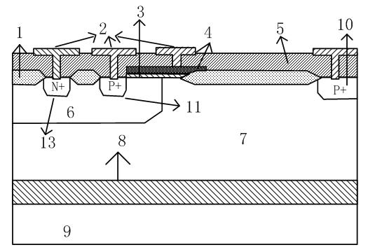
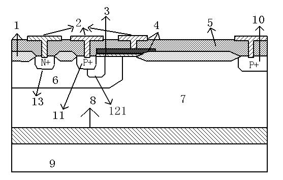
[0017] refer to figure 2 , a high sustain voltage P-type electrostatic protection semiconductor device, comprising: a semiconductor substrate 9, a buried oxide layer 8 is arranged on the semiconductor substrate 9, a P-type doped semiconductor region 7 is arranged on the buried oxide layer 8, and P-type doped semiconductor region 7 is provided with N well 6 and P-type drain region 10, is provided with P-type source region 11 and N-type contact region 13 on N well 6, is provided with gate oxide layer on the surface of N well 6 3 and the gate oxide layer 3 extends from the N well 6 to the P-type doped semiconductor region 7, and the P-type source region 11 on the surface of the N well 6, the N-type contact region 13 and the area other than the gate oxide layer 3 and the P-type doped A field oxide layer 1 is provided in the area other than the P-type drain region 10 on the surface of the semiconductor region 7, and a polysilicon gate 4 is provided on the surface of the gate oxide...


PUM


Abstract

A high-maintenance voltage P-type electrostatic protection semiconductor device, comprising: a semiconductor substrate, a buried oxide layer is arranged on the semiconductor substrate, a P-type doped semiconductor drift region is placed on the buried oxide layer, and the N well region is arranged on Above the P-type doped semiconductor drift region, while the field oxide layer, metal layer, gate oxide layer, polysilicon gate and oxide layer are arranged on the upper surface of the device, and the P-type source region and N-type contact region are arranged in the N well , characterized in that an N-type doped semiconductor region is also provided in the N well, and the N-type doped semiconductor region is located under the P-type source region and the gate oxide layer. The device can effectively increase the holding voltage during electrostatic protection, so the device has better anti-latch-up ability.

Description

technical field [0001] The invention relates to the field of reliability of power semiconductor devices, and more specifically relates to a new structure of a high sustaining voltage semiconductor transistor suitable for electrostatic protection. Background technique [0002] With the increasing demand for energy saving, the performance of power integrated circuit products has attracted more and more attention, and the reliability of the circuit has also attracted more and more attention from circuit design engineers. Electrostatic discharge is a very important reliability issue, and it is also one of the main causes of failure of many electronic products. With the continuous reduction of process feature size, electronic products are more vulnerable to electrostatic discharge damage, so the problem of electrostatic protection has become increasingly severe. [0003] At present, in the problem of electrostatic protection, it is generally on the input and output ports of the ...

Claims


Application Information

Patent Timeline
Patent Type & Authority Applications(China)
IPC IPC(8): H01L29/06H01L29/78
Inventor 钱钦松潘宏伟刘斯扬孙伟锋陆生礼时龙兴
Owner SOUTHEAST UNIV
Why Eureka
Try Eureka