
High-robustness back biased diode applied to high-voltage static protection

A reverse-biased diode, high-voltage electrostatic technology, applied in circuits, electrical components, semiconductor devices, etc., can solve the problems of enlarged devices, low leakage current, and inability to integrate circuits, and achieve the effect of reducing the trigger voltage.

Inactive Publication Date: 2011-07-20
SOUTHEAST UNIV
View PDF7 Cites 4 Cited by
  • Summary
  • Abstract
  • Description
  • Claims
  • Application Information

AI Technical Summary

Problems solved by technology

Transient diodes are the most widely used, and their advantages are fast response time, large transient power, low leakage current, breakdown voltage deviation, easy control of clamping voltage, no damage limit, and small size, but the biggest disadvantage is that they cannot be compared with The circuit is integrated into the same chip, which is a discrete electrostatic protection device
Therefore, people have designed a reverse-biased diode that can be developed in the same process as the circuit at the same time. The biggest disadvantage is that the high electric field after the avalanche makes the secondary breakdown current low because of the high trigger voltage, that is, the robustness of the device. lower sex
In order to increase the secondary breakdown current of the device, the method of increasing the area of ​​the device is often used, which will increase the cost

Method used


Image

  • High-robustness back biased diode applied to high-voltage static protection
  • High-robustness back biased diode applied to high-voltage static protection
  • High-robustness back biased diode applied to high-voltage static protection

Examples


Embodiment Construction

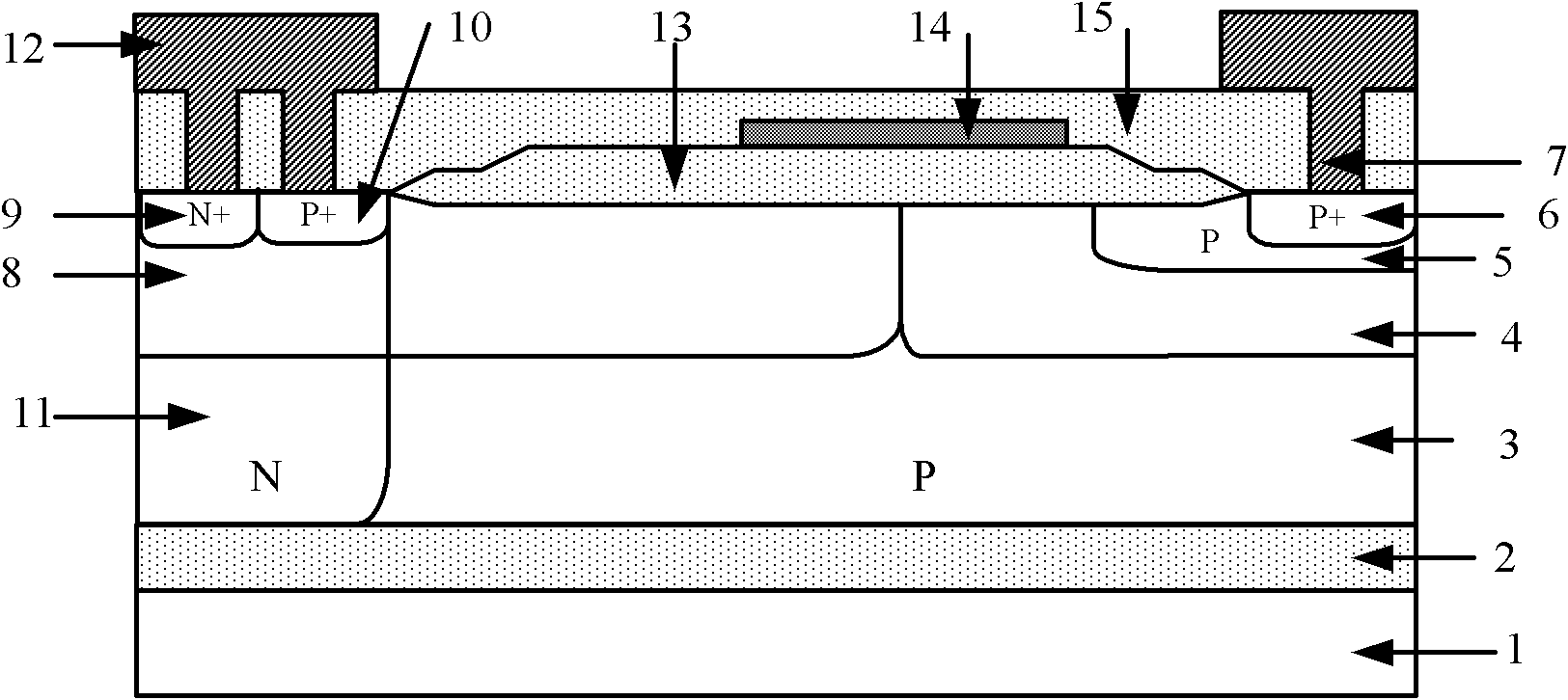
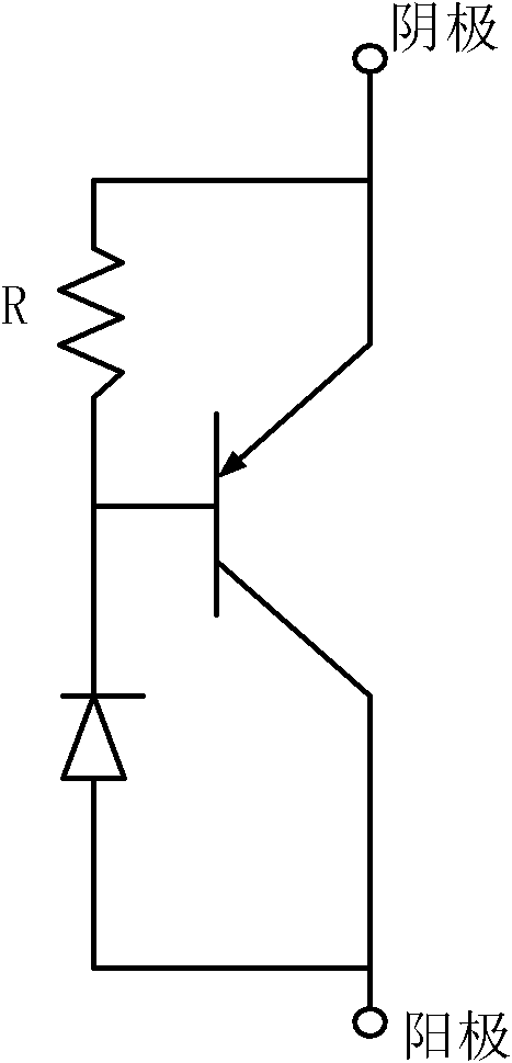
[0027] A highly robust reverse-biased diode applied to high-voltage electrostatic protection, comprising: a P-type substrate 1, a buried oxide layer 2 is arranged on the P-type substrate 1, and a P-type epitaxial layer is arranged on the buried oxide layer 2 3. A first low-voltage P-type well 4, a first low-voltage N-type well 8, and a second high-voltage N-type well 11 are arranged on the upper part of the P-type epitaxial layer 3, and the second high-voltage N-type well 11 is formed from the P-type epitaxial layer. 3 extends to the lower surface of the P-type epitaxial layer 3, a P-type anode region 6 is provided in the first low-voltage P-type well 4, and an N-type cathode region 9 is provided in the second high-voltage N-type well 11. The upper surface of the P-type epitaxial layer 3 is provided with a field oxide layer 13, and the field oxide layer 13 is located between the second high-voltage N-type well 11 and the P-type anode region 6. In the second high-voltage N-type ...


PUM


Abstract

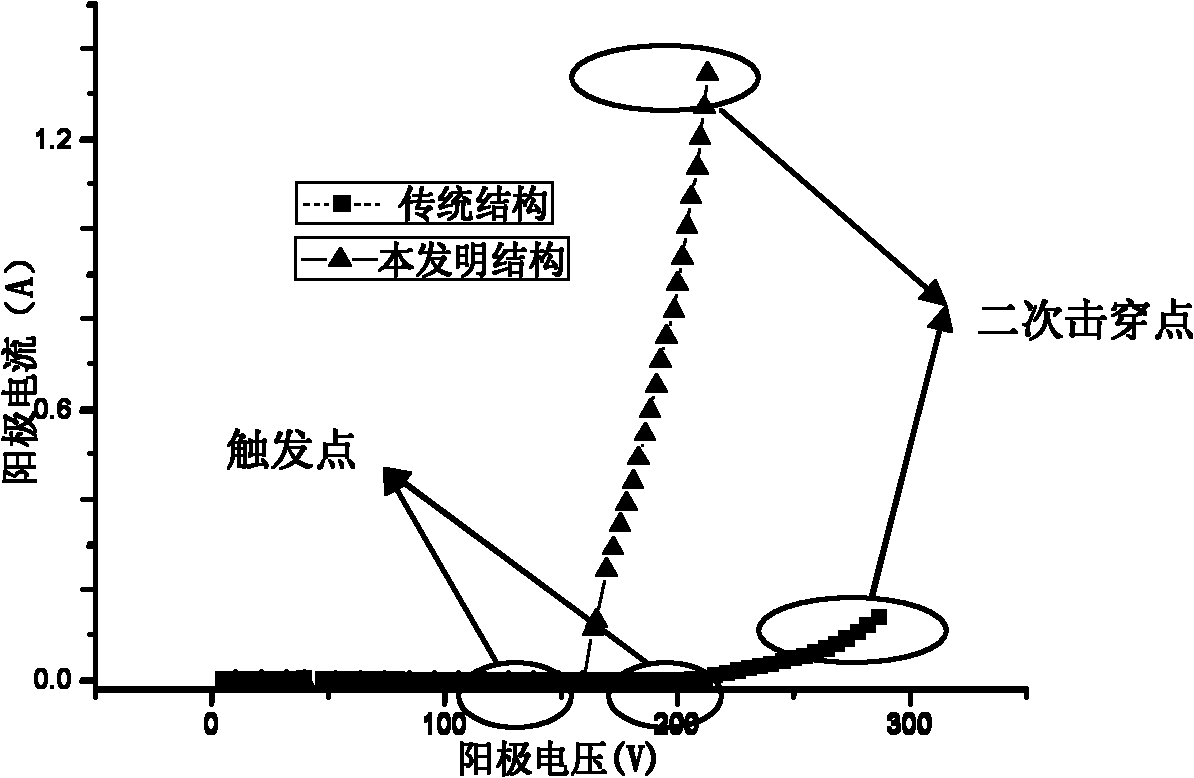
The invention discloses a high-robustness back biased diode applied to high-voltage static protection, comprising a P type substrate, wherein a buried oxide layer is arranged on the P type substrate; a P type epitaxial layer is arranged on the buried oxide layer; a first low-voltage P type well, a first low-voltage N type well and a second high-voltage N type well are arranged at the upper part of the P type epitaxial layer; a P type anode region is arranged in the first low-voltage P type well; an N type cathode region is arranged in the second high-voltage N type well and cathode metal is connected to the N type cathode region; and anode metal is connected to the P type anode region. The high-robustness back biased diode is characterized in that a P type cathode region connected to the cathode metal is arranged on the upper surface inside the second high-voltage N type well and is tightly attached to the right boundary of the N type cathode region; a second P type buffer well is arranged in the first low-voltage P type well; and the P type anode region is positioned in the second P type buffer well. By using the device, the trigger voltage in the static protection process can be effectively reduced and the secondary breakdown current of a lifting device is greatly improved, and thereby the high-robustness back biased diode has better robustness.

Description

technical field [0001] The invention relates to the reliability field of integrated circuits, and relates to a high-robust reverse-biased diode structure suitable for high-voltage electrostatic protection. Background technique [0002] With the increasing demand for energy saving, the performance of power integrated circuit products has attracted more and more attention, and the reliability of the circuit has also attracted more and more attention from circuit design engineers. With the continuous shrinking of the process feature size, how to design an ESD protection device that can realize the ESD protection function without the risk of latch-up on a smaller area has become a major problem in the high-voltage process. [0003] At present, according to the manufacturing process of power integrated circuits, it is mainly divided into bulk silicon-based, epitaxy and silicon-on-insulator (SOI). Among them, the bulk silicon process has many defects in the silicon surface layer,...

Claims


Application Information

Patent Timeline
IPC IPC(8): H01L29/861H01L29/06H01L21/329H01L21/265
Inventor 钱钦松刘斯扬魏守明孙伟锋时龙兴张丽朱奎英
Owner SOUTHEAST UNIV
Learn More