
NLDMOS device, preparation method of NLDMOS device and chip

A device, N-type technology, applied in semiconductor/solid-state device manufacturing, semiconductor devices, electrical components, etc., can solve problems such as optimizing performance

Active Publication Date: 2022-08-05
BEIJING CHIP IDENTIFICATION TECH CO LTD +3
View PDF9 Cites 0 Cited by
  • Summary
  • Abstract
  • Description
  • Claims
  • Application Information

AI Technical Summary

Problems solved by technology

[0003] There are two important parameters to measure the performance of LDMOS devices, namely, the breakdown voltage (BVoff) and on-resistance in the off-state. However, the breakdown voltage (BVoff) in the off-state and the on-resistance are related and contradictory. Therefore, it is impossible to adjust the performance of the two parameters to the best at the same time
Most of the existing technical solutions to improve the performance of LDMOS devices are only designed to improve the breakdown voltage (BVoff) in the off-state under the condition that the on-resistance remains unchanged.

Method used


Image

  • NLDMOS device, preparation method of NLDMOS device and chip
  • NLDMOS device, preparation method of NLDMOS device and chip
  • NLDMOS device, preparation method of NLDMOS device and chip

Examples


Embodiment Construction

[0028] The specific embodiments of the present invention will be described in detail below with reference to the accompanying drawings. It should be understood that the specific embodiments described herein are only used to illustrate and explain the present invention, but not to limit the present invention.

[0029] The Safe Operating Area (SOA) is the current and voltage range within which a power device can operate safely and reliably, outside of which the device may be destroyed. Therefore, when designing the LDMOS structure, in addition to the breakdown voltage and the breakdown voltage (BVoff) in the off state, the inventors also considered another key parameter, that is, the Electrical Safe-operating-area (Electrical Safe-operating-area, The on-state breakdown voltage (BVon) in E-SOA). Among them, the lower limit value and the upper limit value of E-SOA are BVoff and BVon, respectively.

[0030] figure 1 It is a schematic structural diagram of an NLDMOS device provid...


PUM


Abstract

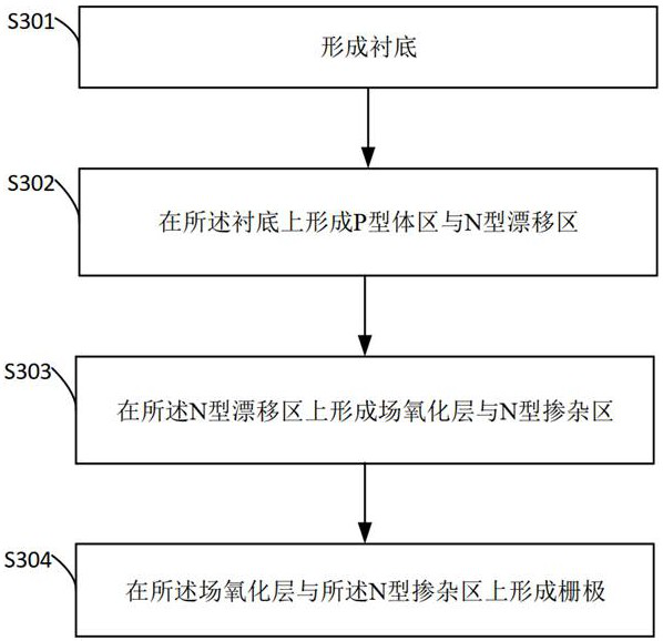
The invention relates to the technical field of semiconductors, and discloses an NLDMOS device, a preparation method of the NLDMOS device and a chip. The NLDMOS device comprises: a substrate; the P-type body region and the N-type drift region are arranged on the substrate; the field oxide layer and the N-type doped region are arranged on the N-type drift region; and the grid electrode is arranged on the field oxide layer and the N-type doped region, and the N-type doped region comprises a junction region of the field oxide layer, the grid electrode and the N-type drift region. According to the invention, the N-type doped region can reduce the on resistance of the NLDMOS device under the condition of ensuring a certain breakdown voltage (BVoff) in a turn-off state, effectively redistributes the power line density so as to reduce the electric field peak value of a junction region, and provides extra net charge for a drift region during large injection of the device, so that the Kirk effect can be effectively inhibited, and the reliability of the device is improved. Therefore, the breakdown voltage (BVon) in a conducting state is improved, namely, the safe working area and the reliability of the NLDMOS device are improved.

Description

technical field [0001] The invention relates to the technical field of semiconductors, in particular to an NLDMOS device, a preparation method of the NLDMOS device and a chip. Background technique [0002] Power management applications account for a large and growing market share, driven by the need for energy efficiency and longer battery life. These needs require a technology that can integrate switches that handle high currents (up to 20A) and high voltages (typically up to 24 or 60V). At present, LDMOS (Laterally Diffused Metal Oxide Semiconductor) device has the characteristics of high voltage resistance, high current driving capability and low power consumption, so it has been widely used as a switching device in the industrial field. [0003] There are two important parameters to measure the performance of LDMOS devices, namely, the breakdown voltage (BVoff) in the off state and the on-resistance. However, the breakdown voltage (BVoff) and the on-resistance in the of...

Claims


Application Information

Patent Timeline
Patent Type & Authority Applications(China)
IPC IPC(8): H01L29/06H01L29/78H01L21/336H01L27/088
CPCH01L29/0615H01L29/0692H01L29/7823H01L29/66681H01L27/088
Inventor 赵东艳王于波陈燕宁吴波刘芳邓永锋王凯余山付振郁文刘倩倩王帅鹏彭鹏邵宇鹰
Owner BEIJING CHIP IDENTIFICATION TECH CO LTD
Learn More