Liquid crystal display device

A liquid crystal display device and liquid crystal layer technology, applied in optics, instruments, electrical components, etc., can solve the problem that the common electrode line cannot meet the requirements of high aperture ratio, and achieve the effects of reducing production cost, simplifying manufacturing process, and improving economic benefits

Active Publication Date: 2013-05-29
NANJING CEC PANDA LCD TECH
View PDF3 Cites 0 Cited by
  • Summary
  • Abstract
  • Description
  • Claims
  • Application Information

AI Technical Summary

Problems solved by technology

[0004] The object of the present invention is to solve the problem that the design of the common electrode line cannot meet the requirement of high aperture ratio in the existing liquid crystal display device, and propose a liquid crystal display device with a pixel array having a high aperture on the first substrate

Method used


Image

  • Liquid crystal display device
  • Liquid crystal display device
  • Liquid crystal display device

Examples


Embodiment 1

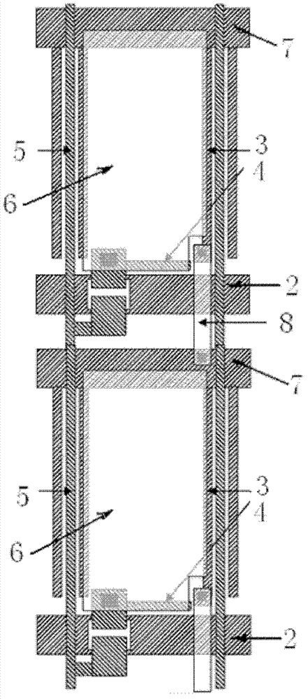
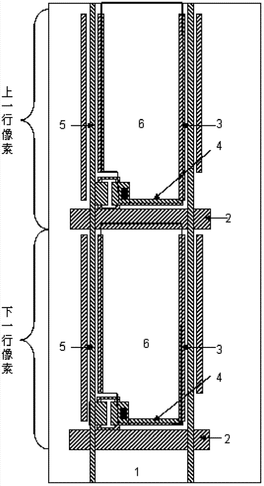
[0042] After adopting the scheme of the present invention, an embodiment of the TN pixel is as follows image 3 shown. For the convenience of description, the figure shows the overall structure of the combination of the upper row of pixels and the lower row of pixels.

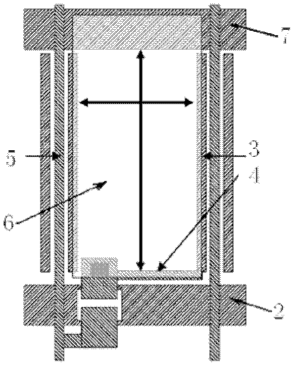
[0043] exist image 3 In , the outermost box surrounding the pixel structure represents the underlying common electrode, which uses transparent materials such as ITO and ZnO. The transparent bottom common electrode is directly formed on the glass substrate by sputtering process. The sheet resistance of the bottom common electrode can be controlled by adjusting sputtering process parameters, film thickness and other items. After the film forming process of the bottom common electrode is completed, a transparent first insulating layer, such as a SiNx layer, SiO2 layer, etc., is then formed. The subsequent manufacturing method is compatible with the existing process: the scanning line 2 pattern, the second ins...

Embodiment 2

[0049] The IPS pixel structure adopting the scheme of the present invention is similar to the pixel structure of FFS, specifically as Figure 6 shown. The difference is that in the FFS pixel structure, the underlying common electrodes are distributed in blocks in each pixel, and the potential of the lower common electrode squares is introduced through the common electrodes.

Embodiment 3

[0051] The VA pixel structure adopting the scheme of the present invention is similar to the TN pixel structure, specifically as Figure 7 shown. The difference is that the pixel electrode 6 of the VA structure is divided into a ">" or "<" shape by the slit 11Slit.

[0052] The potential of the bottom common electrode in the solution of the present invention is introduced at the position of Seal16 outside the display area. Potential introduction position such as Figure 8 As shown: a large-area contact hole 9 is designed around the display area at a position corresponding to the sealing glue Seal16. Through these contact holes 9, the common electrode potential input from the outside of the substrate can be introduced to the bottom common electrode. The specific design embodiment on the position of contact hole 9 can be as follows Figure 9 As shown: the bottom of the contact hole 9 is respectively covered with the metal layer connected to the potential of the common electr...


PUM


Abstract

The invention relates to a liquid crystal display device. A bottom layer common electrode, a first insulating layer, a first metal layer, a second insulating layer, an amorphous silicon layer, a second metal layer, a third insulating layer and a pixel electrode (6) are arranged sequentially from glass of a first substrate to a liquid crystal layer of the first substrate. The bottom layer common electrode is a planar common electrode (1) and is integrally arranged on the glass of the first substrate. In the invention, an overlapping area between the pixel electrode and the common electrode is increased; an adjustable range of a pixel storage capacitance value is improved; a linear metal common electrode line is changed into the planar common electrode made of transparent materials, so thatthe power supply capacity of the common electrode is improved and the potential uniformity at different positions of the common electrode is improved; and by combining light shading lines at both ends of a data line, the pixel aperture opening ratio is improved and a coupling capacitor between the data line and the bottom layer common electrode is reduced. The bottom layer common electrode only needs to be subjected to a sputtering film forming process and does not need to be subjected to a photolithographic process by a special mask plate, so that the production cost is effectively reduced and the economic benefits are improved.

Description

technical field [0001] The invention relates to a liquid crystal display device, especially a display device in which the first substrate has a pixel array with a high opening. Background technique [0002] At present, the existing pixel structures basically use the overlapping of the pixel electrode 6 and the metal common electrode line 7 to form a storage capacitor. The existence of the metal common electrode line 7 reduces the aperture ratio of the pixel. Take the TN pixel structure as an example, such as figure 1 As shown: due to the existence of the common electrode line 7, the pixel opening area is limited to a small space surrounded by the common electrode line 7 and the shielding line. Moreover, in order to increase the storage capacitance of the pixel, it is necessary to increase the overlapping area between the pixel electrode 6 and the common electrode line 7, which requires increasing the width of the common electrode line 7, thereby further reducing the apert...

Claims


Application Information

Patent Timeline
Patent Type & Authority Patents(China)
IPC IPC(8): G02F1/1343G02F1/1362H01L27/12
Inventor 马群刚
Owner NANJING CEC PANDA LCD TECH
Why Eureka
Try Eureka