FPGA-based scalable multi-core processor verification platform
A technology of multi-core processor and verification platform, applied in the field of hardware platform of multi-core processor architecture, can solve the problems of insufficient number of logic units and limited sub-resources of a single board, achieve small area, high PCB utilization rate, and reduce PCB area Effect
- Summary
- Abstract
- Description
- Claims
- Application Information
AI Technical Summary
Problems solved by technology
Method used
Image
Examples
Embodiment 1
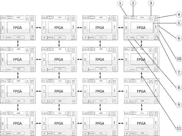
[0034] see figure 1 , this scalable multi-core processor platform based on FPGA, including 16 FPGA development boards, is characterized in that the development board array formed by cascading single FPGA development boards through LVDS interface communicates with each other and cascades into a verification platform .
Embodiment 2
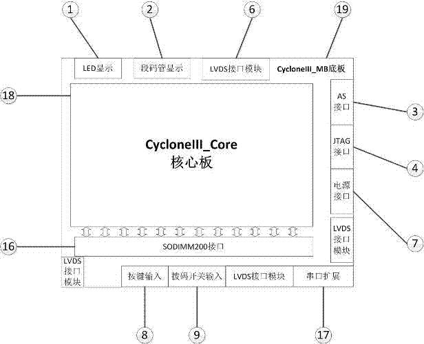
[0036] This FPGA-based scalable multi-core processor verification platform (such as figure 1 As shown) a network structure is formed by a plurality of single development boards (10) through the LVDS connection lines (11) between the development boards; each single development board includes a development board core board (18) and a development board Bottom plate (19) (such as figure 2 shown); the development board bottom plate (19) mainly includes such as figure 2The shown LED display light (1), eight-segment digital tube display (2), AS interface (3), JTAG interface (4), high-speed differential communication interface module (6), power interface (7), ping-pong key input ( 8), DIP switch input (9), SODIMM200 interface (16), extended serial port (17); development board core board (18) mainly includes such as Figure 4 The shown cycloneIII FPGA chip (5), 2 types of frequency crystal oscillator (12), program configuration FLASH (13), off-chip storage device (14), small dual i...
Embodiment 3
[0038] This FPGA-based scalable multi-core processor verification platform is composed of 16 development boards (10), which communicate with each other through LVDS on the bottom board. The following will introduce a single development board in detail:
[0039] (1) Single development board (10)
[0040] A single development board consists of a bottom board (19) and a core board (18), see figure 2 .
[0041] The bottom board mainly includes display output (1) (2), LVDS interface (6), AS interface (3), JTAG interface (4), key input (8) (9), SODIMM200 interface (16).
[0042] The base board and the core board communicate through the SODIMM200 interface (15) (16), and can send the signal on the FPGA chip (5) to the input and output of the base board to realize the control of the development board.
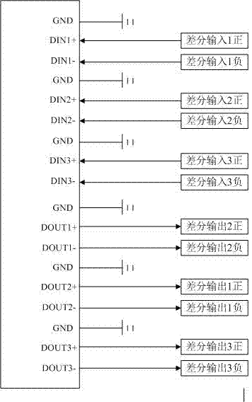
[0043] (2) Backplane LVDS interface (6)
[0044] There are 4 LVDS interfaces (6) on the bottom board, which are respectively placed on the upper, lower, left, and right sides of th...
PUM
 Abstract
Description
Claims
Application Information


