Optical packet switch

a packet switch and optical switch technology, applied in data switching networks, synchronisation signal speed/phase control, multiplex communication, etc., can solve the problems of intra-package clock information capable of being received indiscriminately regardless, devices according to the prior art giving rise, etc., to increase the size and cost of the optical switch, the effect of increasing the size of the devi

Inactive Publication Date: 2003-01-28
NEC CORP
View PDF6 Cites 64 Cited by
  • Summary
  • Abstract
  • Description
  • Claims
  • Application Information

AI Technical Summary

Benefits of technology

There is the third problem as follows. The problem with the device shown in FIG. 10 is that the output interface card 211 is provided with the electrical receiving circuitry for supporting all of the input interface cards 203. In comparison with the arrangements shown in FIGS. 8 and 9, the scale of the electrical receiving circuitry in the output interface card is increased by a factor equivalent to the number (N) of input interface cards and the scale of the electrical circuitry of the overall device also is increased by a factor of N. This results in a much larger device and in higher cost. Furthermore, the number of wavelengths of the optical signals transmitted through the optical switch also is N times the number of wavelengths in the arrangements shown in FIGS. 8 and 9. The result is an increase in the size and cost of the optical switch.
In a packet switch, the relationship between data and retiming clock control information is uniquely determined in each circuit block that resides along the data transfer path within the device. Accordingly, the master clock unit within the device transfers a reference clock to each of the other blocks. By retiming the data in each of the circuit blocks in accordance with a clock phase shifted a fixed length from the reference clock, packets can be sent and received correctly.
Accordingly, an object of the present invention is to provide a packet switch in which electrical circuits are used to implement the input and output sections of an optical switch that performs packet switching, wherein the retiming of packet data in the output section is facilitated and an increase in the scale of the circuitry is suppressed.

Problems solved by technology

Thus, the devices according to the prior art give rise to the following problems:
The first problem is that the device shown in FIG. 8 is disadvantageous in that it is difficult for the output interface card 211 to retime packet-data signals that are transferred from different input interface cards.
The reason for this is that since signal delay or skew is produced that differs depending upon the input interface cards for different sources of transmission, intra-package clock information capable of being received indiscriminately regardless of the particular skew is difficult to be extracted from the master frame signal.
However, difficulty is encountered in the very act of constructing the burst-receiving PLL circuit 230 that extracts the clock dynamically packet by packet at high speeds at an operating frequency on the gigahertz order or greater.
Extracting the clock would take too much time even if such a PLL circuit could be constructed, and it would be impossible to extract a clock and accept data while following up packet transfer on the order of several microseconds or less.
This is the second problem with the prior art.
The problem with the device shown in FIG. 10 is that the output interface card 211 is provided with the electrical receiving circuitry for supporting all of the input interface cards 203.
In comparison with the arrangements shown in FIGS. 8 and 9, the scale of the electrical receiving circuitry in the output interface card is increased by a factor equivalent to the number (N) of input interface cards and the scale of the electrical circuitry of the overall device also is increased by a factor of N. This results in a much larger device and in higher cost.
The result is an increase in the size and cost of the optical switch.

Method used


Image

  • Optical packet switch
  • Optical packet switch
  • Optical packet switch

Examples


examples

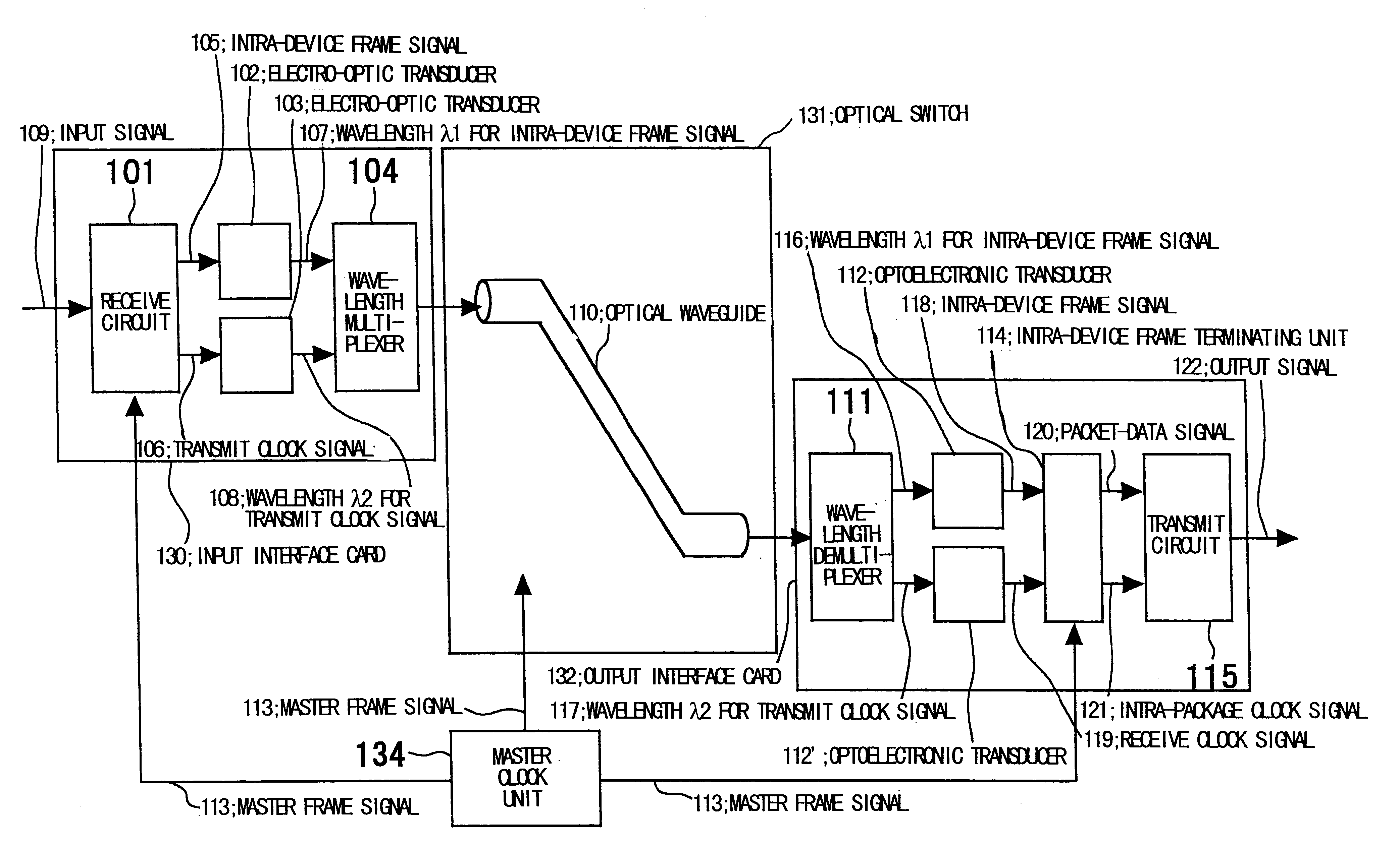
FIG. 4 is a block diagram showing the overall system configuration of an embodiment of an optical packet switch according to the present invention. As shown in FIG. 4, this embodiment includes the input interface card 130, the optical switch 131, the output interface card 132, the master clock unit 134 and the packet scheduler 133.

FIG. 1 is a block diagram illustrating the principal components shown in FIG. 4. As shown in FIG. 1, the input interface card 130 includes the receive circuit 101 for receiving an input signal (an electric signal) 109 from a transmission line, extracting packet data from the payload of the frame, converting this packet data to the format of the intra-device frame, producing the intra-device frame 160 having a length equivalent to the master-frame period based upon the master frame signal 113 from the master clock unit 134, and outputting the intra-device frame signal 105 and transmit clock signal 106; the first and second electro-optic transducers 102, 103...


PUM


Abstract

An optical packet switch uses electric circuits to implement input and output sections of an optical switch that performs packet switching. Retiming of packet data in the output section is facilitated to reduce the scale of the circuitry. In the input section a packet-data signal and a clock signal for retiming the packet data are wavelength multiplexed by a wavelength multiplexer and transferred over the same optical waveguide of the optical switch. In the output section the packet-data signal and the clock signal, which have been transferred from the same optical waveguide in the packet switch, are demultiplexed by a wavelength demultiplexer, and retiming of the packet-data signal is performed by an intra-device frame terminating unit. A frame format comprises, in addition to a flag pattern and a data field, a preamble and dummy data at the beginning and end thereof, respectively, for accommodating skew caused by transfer through the optical switch as well as a period of signal instability produced by switching of the optical switch. The packet data is transferred upon being placed in the data field of the frame format.

Description

This invention relates to an optical packet switch (or switching system) for switching individual packets using an optical switch. More particularly, the invention relates to an optical packet switch in which, without using sophisticated clock synchronizing technology, it is possible to deal with a variation in frame phase due to factors such as skew in an optical switch, thereby making it possible to achieve accurate retiming.Techniques for constructing large-scale packet switches using optical switches are known in the art. However, it is very difficult to perform routing within the switch by referring to packet headers using optical elements alone and to achieve a packet memory using optical elements. For these reasons, packet switches are constructed by combining optical elements with electric circuits. In such a packet switch, the packet switching function is performed by an optical switch and the input / output units of the optical switch are implemented by electric circuits. In...

Claims


Application Information

Patent Timeline
Patent Type & Authority Patents(United States)
IPC IPC(8): H04Q11/00H04L12/931H04B10/00H04B10/27H04L7/10H04L12/70
CPCH04Q11/0005H04Q11/0066H04Q2011/005H04Q2011/0045H04Q2011/0016
Inventor NISHIHARA, MOTOO
Owner NEC CORP
Why Eureka
Try Eureka