Double-gate flash memory device

a flash memory device and double-gate technology, applied in the field of double-gate flash memory devices, can solve the problems of inability to guarantee the retention characteristic of important memories, the scaling down characteristic is worse than that of the cmos device having the same gate length, and the scaling down characteristic of the flash memory device cannot be easily scaled down, so as to improve the scaling down characteristic of the conventional mos type flash memory device and its memory characteristic, and improve the performance and integration density of the flash memory device. ,

Active Publication Date: 2006-02-28
SEOUL NAT UNIV R&DB FOUND
View PDF5 Cites 61 Cited by
  • Summary
  • Abstract
  • Description
  • Claims
  • Application Information

AI Technical Summary

Benefits of technology

[0029]The object of the present invention is to provide a double-gate flash memory device and fabrication method thereof, by introducing a bulk type double-gate flash memory device that is capable of improving the scaling down characteristic of a conventional MOS type flash memory device as well as its memory characteristic and ultimately capable of improving the performance and integration density of a flash memory device.
[0030]Another object of the present invention is to provide a double-gate flash memory device and fabrication method thereof, in which a Fin active region is connected to a bulk silicon substrate by using bulk Si wafer in order to resolve the problems of a conventional SOI device including the floating body effect, the current leakage and the problem of heat conduction towards the SOI silicon substrate, and thus reducing the cost of a wafer.

Problems solved by technology

A conventional metal-oxide semiconductor (MOS) device can easily restrain a short-channel effect by using a thin gate oxide film according to the scaling down, however, a flash memory device cannot be scaled down easily due to non-scalable gate insulators.
However, if the thickness of the tunneling oxide film (66) is reduced, then the important retention characteristic for memory could not be guaranteed.
In an SONOS type flash memory device, however, the thickness of Oxide-Nitride-Oxide (ONO) film, which corresponds to a gate oxide film in a CMOS device, is still thicker than that of the gate oxide film (for example, 2 nm / 4 nm / 4 nm), and thus the scaling down characteristic is worse than that of CMOS device having the same gate length.
Since the trap density is non-uniform, it requires gate length and width over a certain minimum value, and thus it has a limitation in improving integration density.
Since all of the conventional double-gate MOS devices are formed on a SOI substrate, the SOI wafer has the disadvantage of being more expensive than a bulk wafer.
Also, the conventional double-gate MOS devices have the problem of a floating body problem.
Moreover, Buried Oxide (BOX) formed on a SOI silicon substrate (2a) blocks the heat conduction from the device to the SOI silicon substrate (2a), resulting in deterioration of the device characteristic.

Method used


Image

  • Double-gate flash memory device
  • Double-gate flash memory device
  • Double-gate flash memory device

Examples


Embodiment Construction

[0078]Hereinafter, preferred embodiments of the present invention will be described in detail with reference to the accompanying drawings.

[0079]The present invention relates to a flash memory device which has an increased memory capacity through the improvement in integration density by applying the fact that a double-gate device could improve a short channel effect through scaling down of a flash memory device.

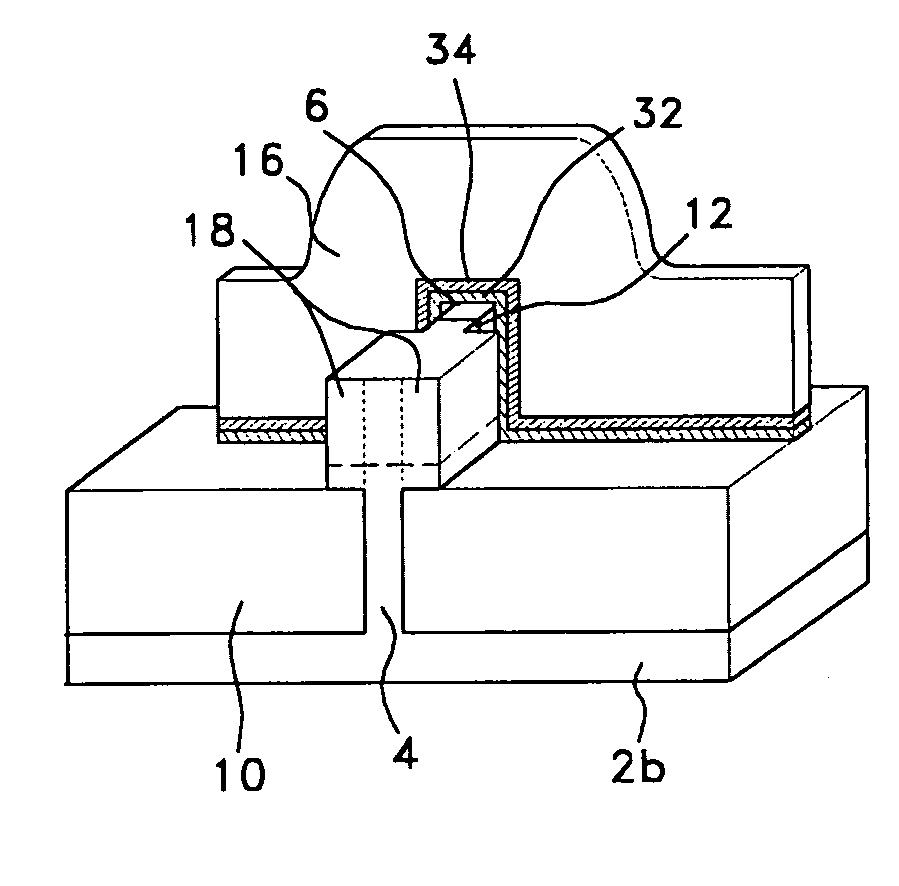
[0080]FIG. 3a is a 3-dimensional diagram which shows the essential parts of a double-gate flash memory device in which a Fin active region of the device is connected to a bulk silicon substrate.

[0081]The diagram shows all the essential parts except the metal layers for wiring and FIG. 3b is a plan view of the device.

[0082]The basic constitution of the double-gate memory flash memory device according to the present invention comprises of: a bulk silicon substrate (2b); a wall-shape single crystal silicon Fin active region (4) which is formed on the upper section of said bulk s...


PUM


Abstract

The conventional flash memory device is fabricated by the MOS processing technology on a bulk substrate and has a similar configuration to an MOS device.While the conventional CMOS device has a superior scaling down characteristic, the scaling down characteristic of a flash memory device is poor due to the inability to reduce the thickness below 7 nm or 8 nm for the tunneling oxide film where the charges in the channel are tunneled into the floating electrode through the tunneling oxide.In order to resolve this problem, the present invention, instead of a SOI wafer, uses a cheaper bulk silicon wafer with lower defect density. A wall shape Fin active region where the channel and the source / drain are formed is connected to the bulk silicon substrate by which floating body effect and heat conduction problem are resolved. a flash memory device is fabricated by forming a tunneling oxide film on side surfaces of the Fin active and a floating (storage) electrode where the charges could be stored.The above structure has a superior scaling down characteristic and enhanced memory performance due to a double-gate flash memory device structure.

Description

BACKGROUND OF THE INVENTION[0001]The present invention relates to a double-gate flash memory device formed on a bulk silicon substrate. More particularly, the invention relates to the structure of a flash memory device which has higher integration density and better program / erase characteristic in comparison to prior art flash memory devices.[0002]A flash memory device has many practical applications, apart from the use in memory itself, it could also be used in various types of electronic apparatus.[0003]A flash memory device is found to be especially suitable for the recently developed embedded logic technology and shows a good process compatibility with the logic technology during the fabrication process.[0004]A highly functional and integrated flash memory device, apart from the use in memory itself, has the potential to bring significant added values in conjunction with logic technology. This fact has attracted a large amount of research activities in this area around the world...

Claims


Application Information

Patent Timeline
Patent Type & Authority Patents(United States)
IPC IPC(8): H01L29/788H01L21/28H01L29/423
CPCB82Y10/00H01L21/28273H01L29/7881H01L29/42324H01L29/42332H01L21/28282H01L29/40114H01L29/40117
Inventor LEE, JONG HO
Owner SEOUL NAT UNIV R&DB FOUND
Why Eureka
Try Eureka