A Transient Voltage Suppressor Based on Zener Diode

A transient voltage suppression, Zener diode technology, applied in the direction of electric solid devices, circuits, electrical components, etc., can solve the problems of loss of ESD protection performance, slow data transmission speed, affecting signal integrity, etc., to achieve short response time , The effect of reducing parasitic capacitance and high surge absorption capacity

Inactive Publication Date: 2011-12-21
ZHEJIANG UNIV
View PDF4 Cites 29 Cited by
  • Summary
  • Abstract
  • Description
  • Claims
  • Application Information

AI Technical Summary

Problems solved by technology

[0008] However, most of the diode structures in traditional TVS are implanted on the P substrate or on the P epitaxy to form a PN junction, relying on a large PN junction area to carry the large ESD current, or injecting P+ on the N substrate or N epitaxy to form a PN junction. Conclusion; At present, traditional TVS is mainly used in portable electronic products such as mobile phones, MP3 and digital cameras. Due to the slow data transmission speed of these products, the requirements for the parasitic capacitance of TVS are not high, and generally allow

Method used


Image

  • A Transient Voltage Suppressor Based on Zener Diode
  • A Transient Voltage Suppressor Based on Zener Diode
  • A Transient Voltage Suppressor Based on Zener Diode

Examples


Embodiment Construction

[0029] In order to describe the present invention more specifically, the technical solution of the present invention and its related principles and manufacturing process will be described in detail below in conjunction with the accompanying drawings and specific embodiments.

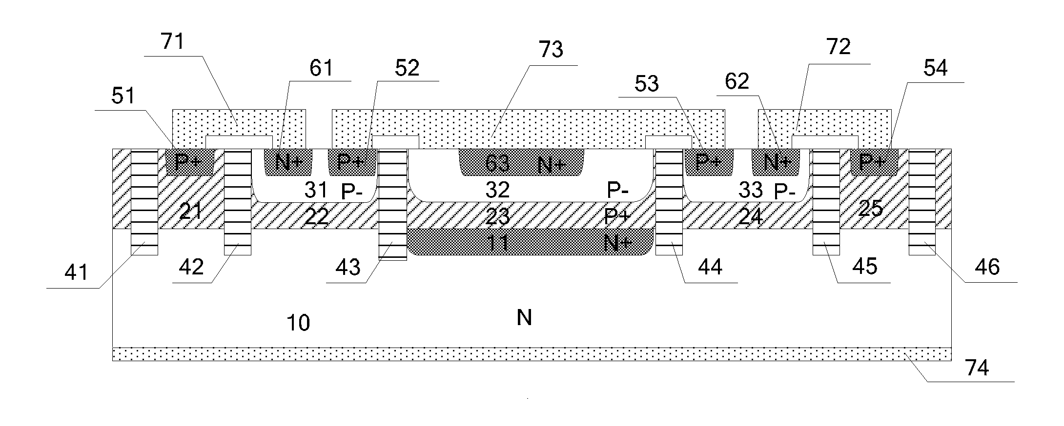
[0030] like figure 1 As shown, a transient voltage suppressor based on a zener diode includes an N substrate layer 10, and the N substrate layer 10 is sequentially provided with a first isolation groove 41, a first P+ epitaxial region 21, and a second isolation groove from left to right. Groove 42, second P+ epitaxial region 22, third isolation trench 43, N+ buried layer 11, fourth isolation trench 44, fourth P+ epitaxial region 24, fifth isolation trench 45, fifth P+ epitaxial region 25, sixth isolation slot 46;

[0031] The second P+ epitaxial region 22 and the fourth P+ epitaxial region 24 are respectively provided with a first P-well 31 and a third P-well 33; the N+ buried layer 11 is sequentially pro...


PUM

PropertyMeasurementUnit
Doping concentrationaaaaaaaaaa
Thicknessaaaaaaaaaa
Doping concentrationaaaaaaaaaa

Abstract

The invention discloses a transient voltage suppressor based on a Zener diode, which comprises an N substrate layer, wherein a first P+ epitaxial region, a second P+ epitaxial region, an N+ buried layer, a four P+ epitaxial region and a fifth P+ epitaxial region are sequentially arranged on the N substrate layer from left to right; a first P- well and a third P- well are respectively arranged on the second P+ epitaxial region and the fourth P+ epitaxial region; a third P+ epitaxial region, a second P- well and a third N+ active injection region are sequentially arranged on the N+ buried layerfrom bottom to top; a first P+ active injection region and a fourth P+ active injection region are respectively arranged on the first P+ epitaxial region and the five P+ epitaxial region; and an N+ active injection region and a P+ active injection area are respectively arranged on the first P-well and the third P-well in a corresponding manner. According to the transient voltage suppressor, the parasitic capacitance of the TVS (Transient Voltage Suppressor) is further reduced by adopting a composite structure of the Zener diode and a low capacity diode; and therefore, the transient voltage suppressor can be widely applied to certain portable equipment and high-speed interfaces for static electricity protection.

Description

technical field [0001] The invention belongs to the technical field of electrostatic protection for integrated circuits, and in particular relates to a transient voltage suppressor based on Zener diodes. Background technique [0002] With the rapid development of electronic information technology, the current semiconductor devices tend to be miniaturized, high-density and multi-functional, especially for applications such as fashion consumer electronics and portable products that have strict requirements on the motherboard area, they are vulnerable to electrostatic discharge (ESD) )Impact. Static electricity exists all the time and everywhere. In the 1960s, with the emergence of MOS devices that are very sensitive to static electricity, the problem of static electricity also appeared. In the 1970s, the problem of static electricity became more and more serious. The density of the circuit is getting bigger and bigger. On the one hand, the thickness of the silicon dioxide fil...

Claims


Application Information

Patent Timeline
IPC IPC(8): H01L27/08
Inventor 董树荣吴健苗萌马飞
Owner ZHEJIANG UNIV
Why Eureka
Try Eureka