A Broadband Low Loss On-Chip Passive Balun with Stacked Serpentine Structure

A low-loss, meandering technology, applied to electrical components, connecting devices, circuits, etc., can solve problems such as deterioration of amplitude balance and phase balance, difficulty in ensuring complete symmetry of geometric structures, and large substrate eddy current effects, etc. Small eddy current effect, reduced substrate eddy current effect, and reduced electromagnetic coupling effect

Active Publication Date: 2011-12-21
SOUTHEAST UNIV
View PDF2 Cites 12 Cited by
  • Summary
  • Abstract
  • Description
  • Claims
  • Application Information

AI Technical Summary

Problems solved by technology

The structure shown in Figure 2(a) is a spiral transformer balun, which has good amplitude balance and phase balance, but the eddy current effect of the substrate is large, resulting in relatively large insertion loss, usually S21<-5dB
Moreover, the geometric structure is relatively complex, and there are intersections between the coils. As shown in Figure 2(b), the crossing wires must be bridged by different layers of metal, which makes it difficult to ensure that the geometric structure is completely symmetrical, which further deteriorates the amplitude balance and phase balance, especially at high The effect of cross section bridging is more serious when frequency

Method used


Image

  • A Broadband Low Loss On-Chip Passive Balun with Stacked Serpentine Structure
  • A Broadband Low Loss On-Chip Passive Balun with Stacked Serpentine Structure
  • A Broadband Low Loss On-Chip Passive Balun with Stacked Serpentine Structure

Examples


Embodiment Construction

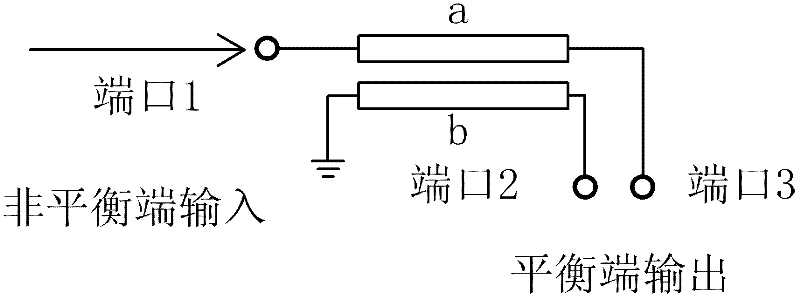
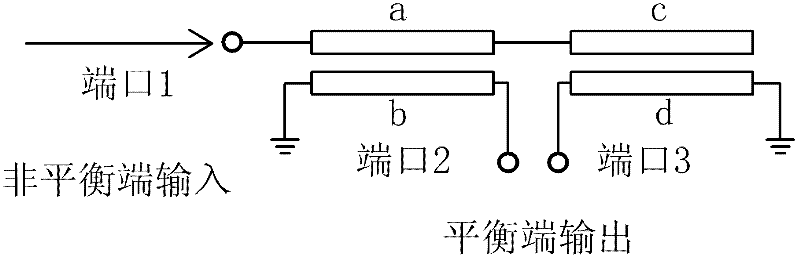
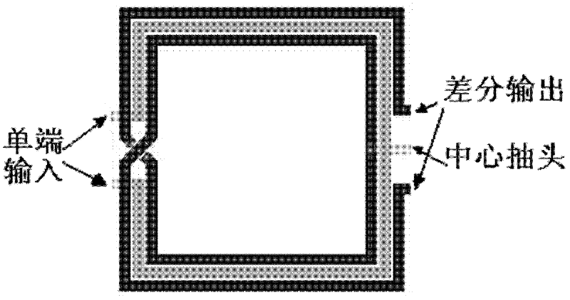
[0027] see Figure 4 , 5 , 6, 7, a passive balun on a laminated meandering structure broadband low-loss chip is provided with three layers of metal wires, an insulating dielectric layer is arranged between each layer of wires, and the first layer of metal wires is a secondary wire, such as Figure 5 shown. The second layer of metal wire is the primary wire, such as Figure 6 shown. The third layer of metal wire is the ground wire, such as Figure 7 shown. The first and last ends of each layer of metal wires are in a U-shaped continuous bending structure (chamfers can be set at the bends), and the geometric structure is completely symmetrical (for the convenience of port leads, the U shape in the middle can be slightly higher) unbalanced The single-ended signal is input to the first end 1 of the primary wire, and the tail end 6 of the primary wire is connected to the ground wire, through the coupling effect of the primary wire and the secondary wire (in order to strengthen...


PUM


Abstract

The invention discloses a broadband low-loss passive balun on chip having a laminated winding structure. The balun on chip is provided with three layers of metal conducting wires. The metal conducting wires in a first layer are secondary conducting wires, the metal conducting wires in a second layer are primary conducting wires and the metal conducting wires in a third layer are ground wires. U-shaped continuous bent winding structures are formed between the heads and tails of the conducting wires of each layer. The geometrical shapes of all U-shaped bends are completely consistent. The U-shaped bends are broken from midpoints between the heads and tails of the secondary conducting wires in the first layer to form left and right discontinuous U-shaped bend sections. Single-end signals of an unbalanced end are connected with the heads of the primary conducting wires. The tails of the primary conducting wires are connected to the ground wires. The heads and tails of the secondary conducting wires are all connected with the ground wires. Breakpoints of the conducting wires in the same sections with the heads of the secondary conducting wires are normal phase signal output ends, and the breakpoints of the conducting wires in the same sections with the tails of the secondary conducting wires are inverted signal output ends. The single-end signals of the unbalanced end are convertedinto differential signals of a balanced end for output under the coupling action of the primary and secondary conducting wires. The ground wires reduce the insertion loss of the balun and simultaneously expand a gain bandwidth and a matched bandwidth.

Description

technical field [0001] The invention relates to a broadband passive balun, in particular to a broadband low-loss on-chip passive balun with a laminated meandering structure, which is suitable for millimeter wave circuits. Background technique [0002] In wireless receiving and transmitting systems, it is usually necessary to use a balun to convert single-ended signals to differential signals. For example, convert the single-ended signal received by the antenna into a differential signal and connect it to a low noise amplifier, or convert the differential signal into a single-ended signal and connect it to the antenna for transmission. Balun is a circuit device that completes the conversion function of single-ended signal and differential signal. The difficulty in its design lies in how to ensure good amplitude balance, phase balance and low insertion loss. [0003] Traditional structure baluns are mainly Marchand structure baluns and spiral structure transformer baluns. Th...

Claims


Application Information

Patent Timeline
Patent Type & Authority Applications(China)
IPC IPC(8): H01P5/10
Inventor 李智群曹佳李芹王志功
Owner SOUTHEAST UNIV
Why Eureka
Try Eureka