Check patentability & draft patents in minutes with Patsnap Eureka AI!

Method for fabricating metal oxide semiconductor device with epitaxially grown stress-induced source and drain regions

A stress-induced, semiconductor technology, applied in semiconductor/solid-state device manufacturing, electrical components, circuits, etc., to solve problems such as increased possibility of channel contamination, recession, etc.

Inactive Publication Date: 2011-12-21
GLOBALFOUNDRIES INC
View PDF4 Cites 6 Cited by
  • Summary
  • Abstract
  • Description
  • Claims
  • Application Information

AI Technical Summary

Problems solved by technology

However, as the thickness of these films decreases with device pitch, the applied stress, and thus the performance benefit achieved, also decays with each new generation
Furthermore, as the thickness of the gate stack decreases in advanced devices, the possibility of channel contamination by impurity dopants from high energy ion implantation processes increases

Method used


Image

  • Method for fabricating metal oxide semiconductor device with epitaxially grown stress-induced source and drain regions
  • Method for fabricating metal oxide semiconductor device with epitaxially grown stress-induced source and drain regions
  • Method for fabricating metal oxide semiconductor device with epitaxially grown stress-induced source and drain regions

Examples


Embodiment Construction

[0009] The following detailed description of the invention is merely exemplary in nature and is not intended to limit the invention or the application and uses of the invention. Furthermore, there is no intention to be bound by any theory presented in the preceding background or the following embodiments.

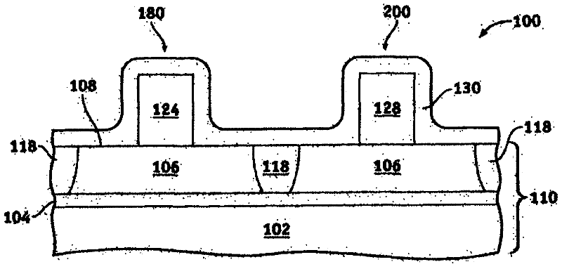
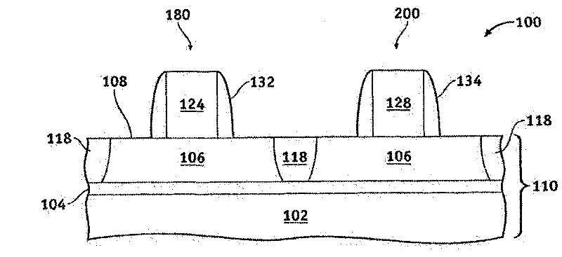
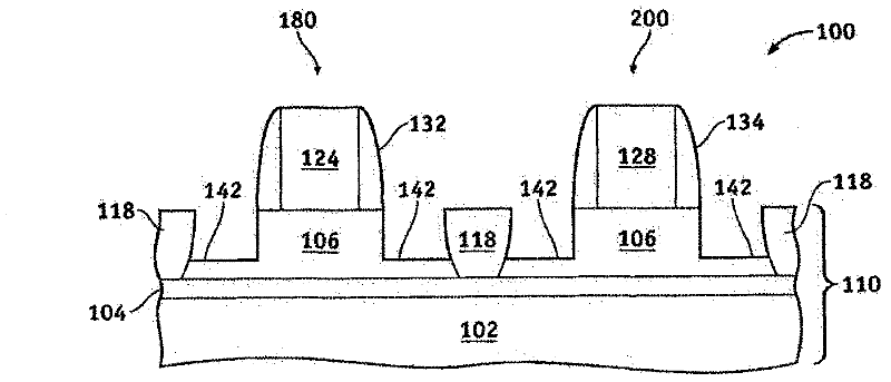
[0010] Historically, epitaxially forming regions for source and drain regions of NFET and PFET devices involved separate sets of process steps for each device type. After forming the gate stacks in both the PFET and NFET regions, the first set of process steps are then used to form the source and drain of one of these device types. In this sequence, a second set of similar steps is followed to form the source and drain of another device type. Each set of process steps typically includes: 1) depositing a blanket dielectric layer in both the PFET and NFET regions, 2) lithographically forming a soft mask to cover the first ( PFET or NFET region), 3) anisotropically etch the ...


PUM


Abstract

The invention provides a method of manufacturing a semiconductor device (100) on and in a semiconductor substrate (110) having a first region (180) and a second region (200). According to an exemplary embodiment of the present invention, a method includes: forming a first gate stack (124) overlying the first region (180) and a second gate stack (128) overlying the second region (200); etching a first recess (142) and a second recess (142) into the substrate (110), the first recess (142) being at least aligned with the first recess in the first region (180) a gate stack (124), and the second recess (142) is aligned at least with the second gate stack (128) in the second region (200); epitaxially growing a first stress-inducing single crystal material (150 ) in the first and second recesses (142); removing the first stress-inducing single crystal material (150) from the first recess (142); and epitaxially growing a second stress-inducing single crystal material (170) in In the first recess (142); wherein the second stress-inducing single-crystal material (170) has a composition different from that of the first stress-inducing single-crystal material (150).

Description

technical field [0001] The present invention relates generally to methods of fabricating semiconductor devices, and more particularly to methods of fabricating metal oxide semiconductor devices having epitaxially grown stress-inducing source and drain regions. Background technique [0002] Most of today's integrated circuits (ICs) are implemented using a plurality of interconnected field effect transistors (FETs), also known as metal oxide semiconductor field effect transistors (MOSFETs or MOS transistors). Generally, both P-channel and N-channel FETs are used to form an IC, and in this case, the IC is called a complementary MOS or CMOS IC. There is a continuing trend to add more and more complex circuits onto a single IC chip. To continue this trend, the size of each individual device in a circuit and the spacing, or pitch, between device components is shrinking with each new technology generation. Furthermore, as the pitch shrinks to smaller dimensions, the thicknesses o...

Claims


Application Information

Patent Timeline
Patent Type & Authority Applications(China)
IPC IPC(8): H01L21/8234H01L21/8238
CPCH01L21/823814H01L21/823418H01L21/823412H01L21/823807H01L21/84H01L29/66712
Inventor R·波尔F·B·杨
Owner GLOBALFOUNDRIES INC
Features
  • R&D
  • Intellectual Property
  • Life Sciences
  • Materials
  • Tech Scout
  • Unparalleled Data Quality
  • Higher Quality Content
  • 60% Fewer Hallucinations
Learn More