Preparation method of organic solar cell and organic solar cell prepared therefrom
A solar cell and organic technology, applied in the field of solar cells, achieves the effects of low cost, favorable promotion and application, and simplified preparation process
- Summary
- Abstract
- Description
- Claims
- Application Information
AI Technical Summary
Problems solved by technology
Method used
Image


Examples
preparation example Construction
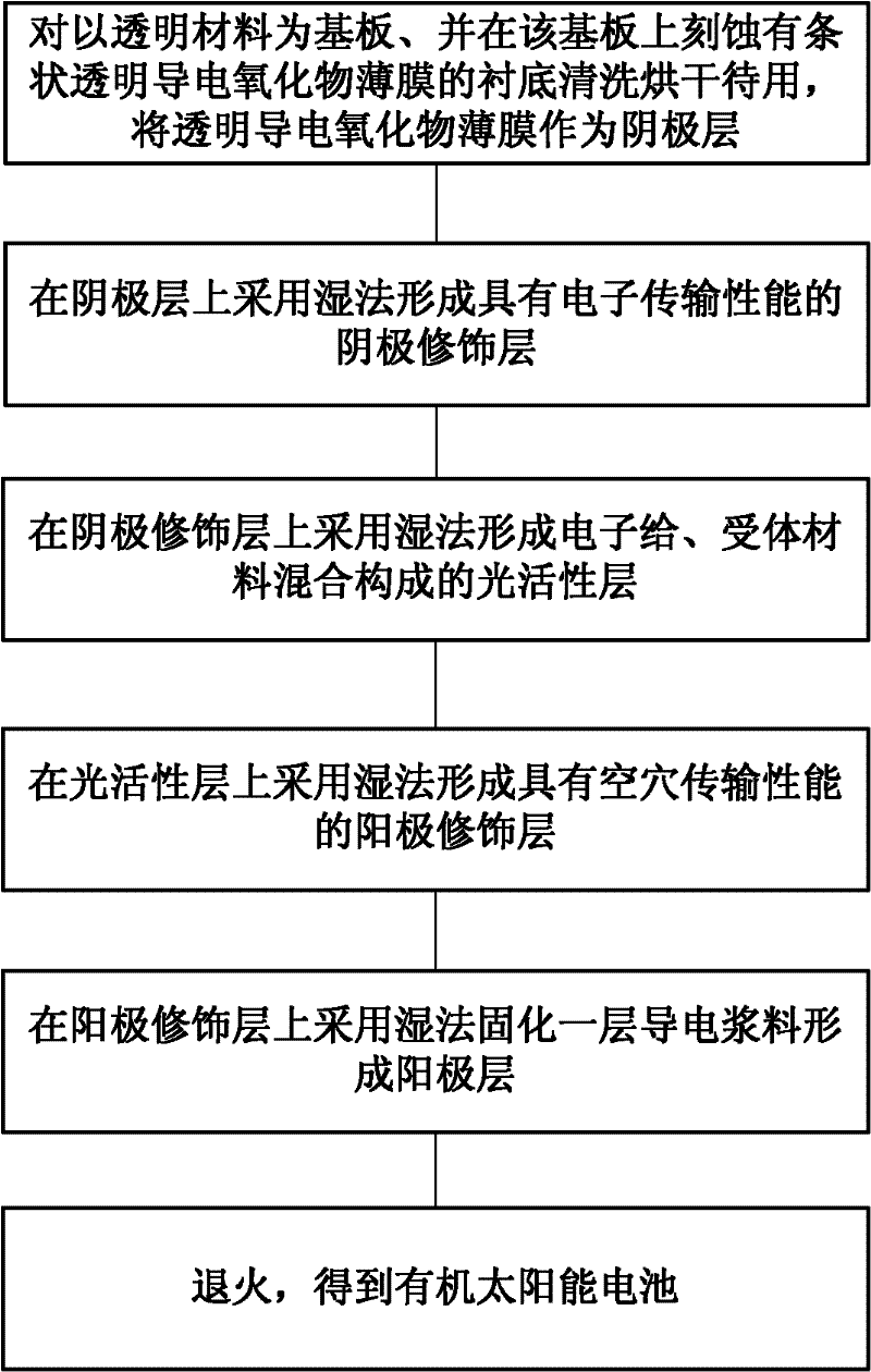
[0043] figure 2 It is a flowchart of the preparation method of the organic solar cell of the present invention. Such as figure 2 As shown, in the preparation method of the present invention, all adopt the wet method to prepare each layer of the organic solar cell:
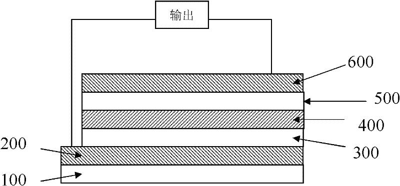
[0044] Clean and dry the substrate with a transparent material as the substrate and etched a strip-shaped transparent conductive oxide film on the substrate, and use the transparent conductive oxide film on the substrate as the cathode layer; in the above The transparent conductive oxide film is prepared by wet methods such as sol-gel method, spin coating method, screen printing method, inkjet printing method, spraying method, etc. to form a cathode modification layer with electron transport properties;
[0045] Then, on the cathode modification layer prepared in the previous step, the electron donor material and the electron acceptor material are deposited by wet methods such as sol-gel method, spin coating me...
Embodiment 1
[0049] (1) On the glass substrate, utilize the sol-gel method to prepare the ITO transparent conductive film that thickness is 80nm, and etch into the thin strip shape with certain width, clean and dry stand-by;
[0050] (2) The ZnO nanoparticles prepared by the sol-gel method are dispersed in chlorobenzene, and the concentration is 50mg / mL, and then spin-coated on the ITO transparent conductive film, and the speed of the homogenizer is 4500rpm (rev / min), uniform The glue time is 30s, forming a layer of ZnO with a thickness of 20nm, and heating at 180°C for 35min to solidify, then cooling;
[0051] (3) On the ZnO layer, add dropwise the chlorobenzene solution containing P3HT and PCBM with a mass ratio of 4: 1, uniformly mixed, and a total concentration of 15 mg / mL. Obtain a photoactive layer with a thickness of 60nm, place it in a glove box, heat at 120°C for 15min to solidify, and cool;
[0052] (4) Spin-coat a PEDOT:PSS layer on the photoactive layer, control the speed of t...
Embodiment 2
[0056] (1) On the silicon substrate, the AZO transparent conductive film with a thickness of 100nm is prepared by the sol-gel method, and etched into thin strips with a certain width, cleaned and dried for use;
[0057] (2) Prepare a layer of TiO with a thickness of 40nm on the AZO transparent conductive film by sol-gel method 2 , and heated at 200°C for 20 minutes to solidify, then cooled;
[0058] (3) on TiO 2 On the layer, a chlorobenzene solution containing P3HT and PCBM with a mass ratio of 2:1, uniformly mixed, and a total concentration of 18 mg / mL was added dropwise, and a photoactive layer with a thickness of 200 nm was prepared by inkjet printing and placed in a glove box. Heating at 100°C for 25 minutes to solidify, then cooling;
[0059] (4) Disperse NiO nanoparticles in dichloromethane, print a layer of NiO with a thickness of 60nm on the active layer by screen printing, heat at 50°C for 15min to solidify, and cool;
[0060] (5) Utilize spraying method to form o...
PUM
| Property | Measurement | Unit |
|---|---|---|
| Thickness | aaaaa | aaaaa |
| Thickness | aaaaa | aaaaa |
| Thickness | aaaaa | aaaaa |
Abstract
Description
Claims
Application Information
 - R&D Engineer
- R&D Manager
- IP Professional
- Industry Leading Data Capabilities
- Powerful AI technology
- Patent DNA Extraction
Browse by: Latest US Patents, China's latest patents, Technical Efficacy Thesaurus, Application Domain, Technology Topic.
© 2024 PatSnap. All rights reserved.Legal|Privacy policy|Modern Slavery Act Transparency Statement|Sitemap