Drilling process of induction magnetic ring plate
A manufacturing process and induction magnetic ring technology, applied in the direction of printed circuit manufacturing, electrical components, printed circuits, etc., can solve the problems of easy wire drawing, high cost, waste of resources, etc., achieve fiber cutting and chip removal improvement, reduce costs, The effect of promoting
- Summary
- Abstract
- Description
- Claims
- Application Information
AI Technical Summary
Problems solved by technology
Method used
Image
Examples
Embodiment Construction
[0029] The present invention is described in further detail below with preferred embodiment:
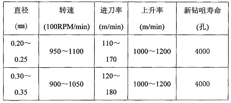
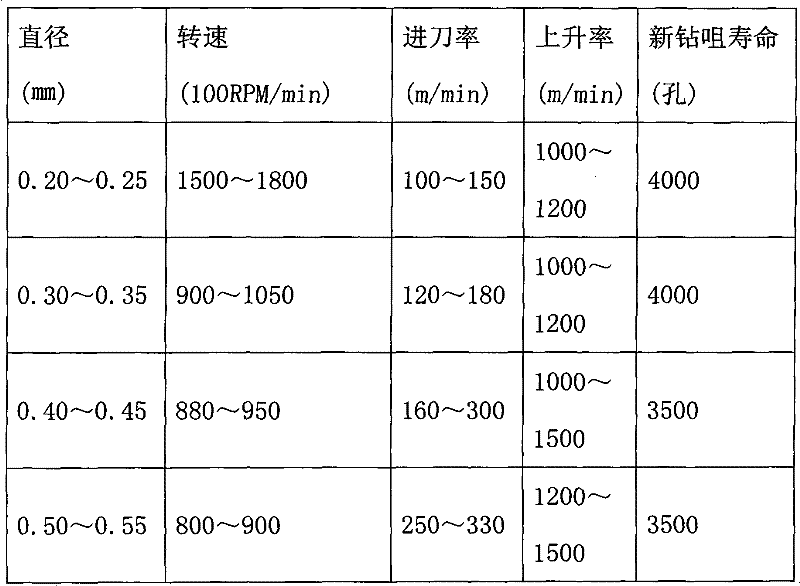
[0030] The thin plate aperture (0.25mm) hole and hole spacing of the present invention is 0.25mm (per m 2 The holes are more than 1,000,000) to produce boards, and the hole thickness and wicking effect are changed. The original hole thickness is controlled below 30um, and the wicking effect is controlled within 1mil. After the design, the hole thickness control is below 10um, and the wicking effect is controlled within 0.05mil. To meet the above requirements, the material and parameters need to be modified.
[0031] For the design change of the inner core board, complete the layout design of the PCB inner layer through the existing circuit board auxiliary software, modify the line width and hole spacing, select and delete the independent PAD to ensure uniform glue flow during lamination, and A square flow blocking block is designed on the inner process side, and at the same time, it...
PUM
 Abstract
Description
Claims
Application Information


