

Wafer Handling Deposition Shield Components
A process chamber, cylindrical technology used in the field of wafer processing deposition shielding components, which can solve problems such as uneven deposition
- Summary
- Abstract
- Description
- Claims
- Application Information
AI Technical Summary
Problems solved by technology
Method used
Image

Examples
Embodiment Construction
[0027] Embodiments described herein provide apparatus and methods for uniformly depositing sputtered material across high aspect ratio features of a substrate during the fabrication of integrated circuits on the substrate.
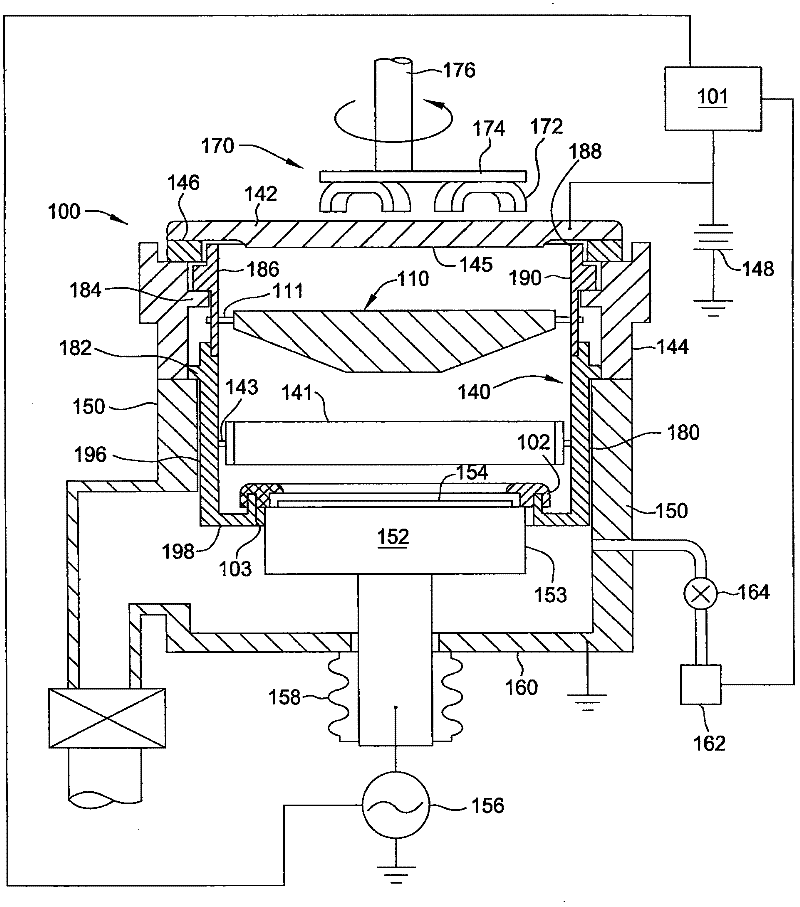
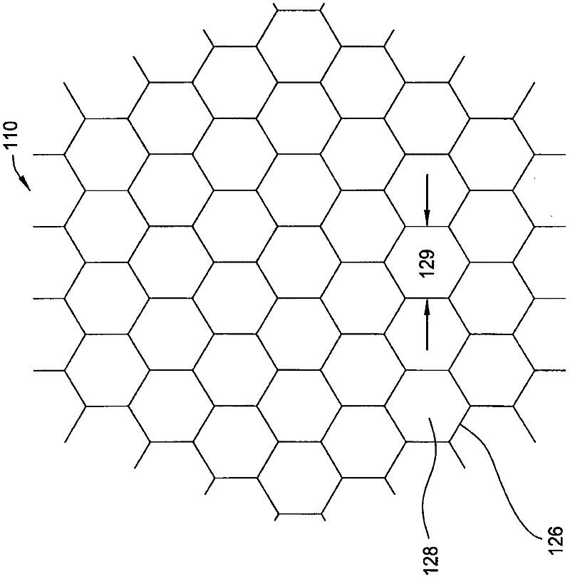
[0028] figure 1 An example embodiment of a processing chamber 100 having one embodiment of a processing kit 140 that can process a substrate 154 is shown. The processing kit 140 includes a one-piece lower shield 180 , a one-piece upper shield 186 and a collimator 110 . In the illustrated embodiment, the processing chamber 100 comprises a sputtering chamber, also known as a It is a physical vapor deposition (PVD) chamber. Examples of suitable PVD chambers include the ALPS, both available from Applied Materials, Inc., Santa Clara, California. Plus and SIP ENCORE PVD processing chamber. It should be appreciated that processing chambers from other manufacturers may also be utilized to practice the embodiments described herein.
[0029] The chamber 100 ...
PUM
 Abstract
Description
Claims
Application Information