Isolation structure of high voltage driver circuit

一种高压驱动电路、隔离结构的技术,应用在电路、电气元件、半导体器件等方向,能够解决P型结隔离区不能完全耗尽、击穿等问题,达到灵活性大、制备简单的效果

Inactive Publication Date: 2012-01-04
SOUTHEAST UNIV
View PDF5 Cites 17 Cited by
  • Summary
  • Abstract
  • Description
  • Claims
  • Application Information

AI Technical Summary

Problems solved by technology

[0004] The invention provides an isolation structure for a high-voltage drive circuit. The invention solves the problem of local breakdown caused by the incomplete depletion of the P-type junction isolation area far away from the high-voltage area, and improves the withstand voltage of the isolation structure.

Method used


Image

  • Isolation structure of high voltage driver circuit
  • Isolation structure of high voltage driver circuit
  • Isolation structure of high voltage driver circuit

Examples


Embodiment 1

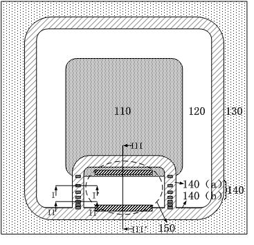
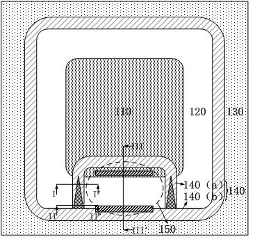
[0024] An isolation structure for a high-voltage driving circuit, comprising: a P-type substrate 1, a P-type epitaxial layer 2 is arranged on the P-type substrate 1, a low-voltage region 130 and a high-voltage region 110 are arranged on the P-type epitaxial layer 2, and the Between the low-voltage region 130 and the high-voltage region 110, there is a high-low voltage junction termination region 120, and between the high-voltage and low-voltage junction termination region 120 and the low-voltage region 130 is a first P-type junction isolation region 140a. The first P-type junction isolation The region 140a is composed of the P-type buried layer 4 and the first P-type well region 71, and a second P-type junction isolation region 140b is provided in the inner region of the first P-type junction isolation region 140a, and the second P-type junction isolation region 140b is connected to the first P-type junction isolation region 140a. The first P-type junction isolation region 140a...

Embodiment 2

[0026] An isolation structure for a high-voltage driving circuit, comprising: a P-type substrate 1, a P-type epitaxial layer 2 is arranged on the P-type substrate 1, a low-voltage region 130 and a high-voltage region 110 are arranged on the P-type epitaxial layer 2, and the Between the low-voltage region 130 and the high-voltage region 110, there is a high-low voltage junction termination region 120, and between the high-voltage and low-voltage junction termination region 120 and the low-voltage region 130 is a first P-type junction isolation region 140a. The first P-type junction isolation The region 140a is composed of the P-type buried layer 4 and the first P-type well region 71, and a second P-type junction isolation region 140b is provided in the inner region of the first P-type junction isolation region 140a, and the second P-type junction isolation region 140b is connected to the first P-type junction isolation region 140a. The first P-type junction isolation region 140a...

Embodiment 3

[0028] An isolation structure for a high-voltage driving circuit, comprising: a P-type substrate 1, a P-type epitaxial layer 2 is arranged on the P-type substrate 1, a low-voltage region 130 and a high-voltage region 110 are arranged on the P-type epitaxial layer 2, and the Between the low-voltage region 130 and the high-voltage region 110, there is a high-low voltage junction termination region 120, and between the high-voltage and low-voltage junction termination region 120 and the low-voltage region 130 is a first P-type junction isolation region 140a. The first P-type junction isolation The region 140a is composed of the P-type buried layer 4 and the first P-type well region 71, and a second P-type junction isolation region 140b is provided in the inner region of the first P-type junction isolation region 140a, and the second P-type junction isolation region 140b is connected to the first P-type junction isolation region 140a. The first P-type junction isolation region 140a...


PUM


Abstract

The invention relates to an isolation structure of a high voltage driver circuit. The isolation structure is characterized in that: the structure comprises a P type substrate and a P type epitaxial layer; a high voltage area, a low voltage area and a high and low voltage junction terminal area are arranged on the P type epitaxial layer; a first P type junction isolation area is arranged between the high and low voltage junction terminal area and the low voltage area as well as a high voltage insulated gate field effect tube is arranged between the high voltage area and the low voltage area; two sides of the high voltage insulated gate field effect tube and an isolation structure between the high voltage insulated gate field effect tube and a high side area are formed into a second P type junction isolation area.

Description

technical field [0001] The invention relates to a high-voltage half-bridge gate drive circuit in a high-voltage power integrated circuit, and relates to an isolation structure in an integrated high-voltage drive circuit. Background technique [0002] High voltage gate drive circuits are used in various fields such as motor drives, electronic rectifiers in fluorescent lamps, and power management. The level shift circuit in the high voltage gate drive circuit is the key part of the whole circuit. The electrical performance of the high voltage insulated gate field effect transistor LDMOS and the electrical coupling between the high voltage LDMOS that make up the level shift circuit will affect the performance of the shift circuit. The high voltage LDMOS source The large current and high voltage at the terminal and drain terminals will also cause parasitic effects in other areas of the entire integrated circuit and thus affect the electrical performance of the entire integrated ...

Claims


Application Information

Patent Timeline
Patent Type & Authority Applications(China)
IPC IPC(8): H01L29/06H01L29/78
CPCH01L29/0847H01L29/7835H01L21/265H01L21/761H01L29/78H01L29/1083H01L29/0692H01L29/0646H01L21/823481
Inventor 时龙兴钱钦松孙伟锋祝靖黄贤国陆生礼
Owner SOUTHEAST UNIV
Why Eureka
Try Eureka