Characterization method for parasitical bipolar junction transistor of MOS (metal oxide semiconductor) transistor
A technology of MOS transistor and bipolar transistor, which is applied in the field of characteristic characterization of parasitic BJT, can solve the problems of complicated testing process, and achieve the effect of simplifying the testing process.
- Summary
- Abstract
- Description
- Claims
- Application Information
AI Technical Summary
Problems solved by technology
Method used
Image

Examples
Embodiment Construction
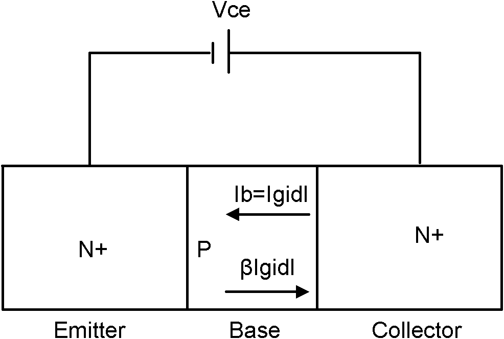
[0020] The test method of the present invention calculates the current gain coefficient β of the parasitic bipolar transistor in the MOS transistor by measuring the gate-induced drain leakage current Igidl of the MOS transistor, thereby generating the current gain coefficient β and the source electrode and the drain electrode of the MOS transistor. The voltage Vds of the parasitic bipolar transistor, that is, the fitting function of the voltage Vce between the emitter and collector of the parasitic bipolar transistor, does not need to contact the body region of the MOS transistor. In order to make the object, technical solution and advantages of the present invention clearer, the present invention will be further described in detail below in conjunction with the accompanying drawings.
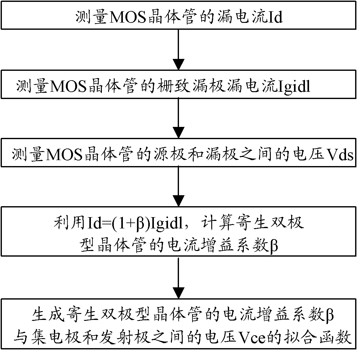
[0021] see image 3 , image 3 is a flow chart of the testing method of the present invention. Preferably, the MOS transistor is a lateral SOI structure MOS transistor, and the parasitic bipo...
PUM
 Abstract
Description
Claims
Application Information