Method for making copper cylinder on circuit board and circuit board with surface copper cylinders

A circuit board and copper column technology, which is applied in the direction of multi-layer circuit manufacturing, printed circuit components, electrical connection printed components, etc. Application and other problems, to achieve the effect of not easy to break and fall off

Active Publication Date: 2012-01-18
SHENNAN CIRCUITS
View PDF2 Cites 14 Cited by
  • Summary
  • Abstract
  • Description
  • Claims
  • Application Information

AI Technical Summary

Problems solved by technology

Due to the uneven current density during electroplating, the electroplated copper pillars are uneven, and the dry film on the surface of the substrate cannot be leveled. Therefore, the copper pillars produced by this method cannot meet the requirements of modern soldering and packaging.
In addition, since the electroplated copper pillars protrude from the surface of the substrate, they cannot be effectively protected during subsequent processing and are easy to fall off; it is also difficult to make circuit patterns on the substrate surface where the copper pillars are formed, and the substrate space cannot be effectively used
Based on the above series of problems, the process of bump welding by welding copper pillars cannot be applied and promoted

Method used


Image

  • Method for making copper cylinder on circuit board and circuit board with surface copper cylinders
  • Method for making copper cylinder on circuit board and circuit board with surface copper cylinders
  • Method for making copper cylinder on circuit board and circuit board with surface copper cylinders

Examples


other Embodiment approach

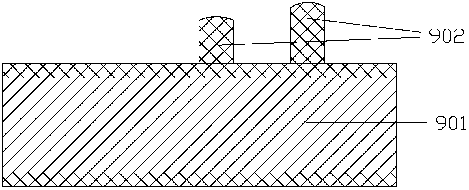
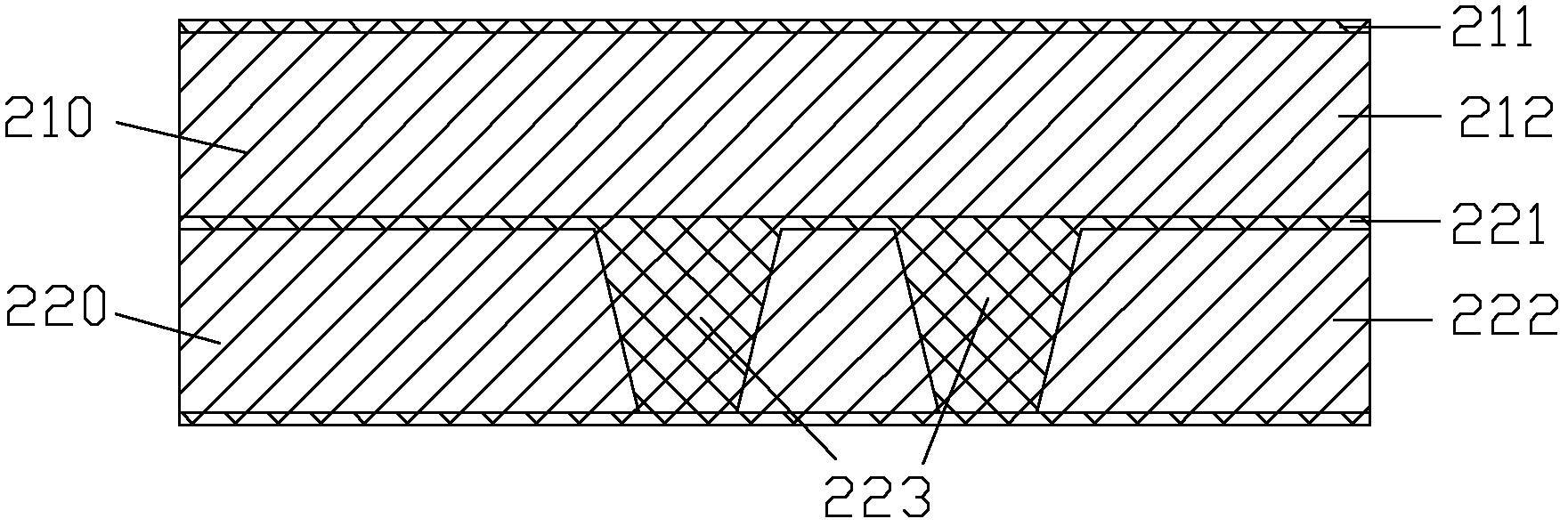
[0020] In other embodiments, when it is necessary to electrically connect the mounted flip chip with the circuit patterns of other layers within the second outer layer, the first blind hole 213 can be connected to the multi-layer when making the first blind hole 213. The second blind hole 223 in the sub-outer layer 220 of the substrate is a solid conductive blind hole filled and leveled by electroplating.

[0021] In this case, before making the first blind hole 213, at least one second blind hole 223 should be made in the second outer layer 220 according to the flip chip to be packaged, and the second blind hole 223 should be filled by electroplating. The blind hole 223 makes it a solid conductive blind hole. It is easy to understand that the first blind holes 213 and the second blind holes 223 may have a one-to-one correspondence, and each first blind hole 213 is connected to a corresponding second blind hole 223 .

[0022] 102. Electroplating fills up the first blind hole,...


PUM


Abstract

The embodiment of the invention discloses a method for making copper cylinders on a circuit board, comprising the following steps: making first blind holes on the outermost layer of a multilayer substrate; filling and leveling up the first blind holes through galvanizing so as to form the copper cylinders, which can be connected with the second outermost layer of the multilayer substrate, in the first blind holes; and removing the outermost layer at a certain area and depth around the first blind holes through laser ablation to keep the copper cylinders formed in the first blind holes. The embodiment of the invention also provides a corresponding circuit board with surface copper cylinders. By the method disclosed by the embodiment of the invention, the copper cylinders are formed on the outermost layer of the multilayer substrate, the height of the copper cylinders can be kept consistent, the copper cylinders are firm and reliable and cannot be broken or fall off easily, and the operation that a circuit graph is made on a substrate surface is not influenced.

Description

technical field [0001] The invention relates to the technical field of circuit board production, in particular to a method for manufacturing copper pillars on a circuit board and a circuit board with surface copper pillars. Background technique [0002] Packaging technology has higher and higher requirements for soldering. As flip-chip technology has become the current mainstream technology, high-density soldering between chips and packaging substrates has become a key research object. Since the solder joints are getting smaller and smaller, in order to improve the soldering yield and reliability, it is proposed to replace the original plane soldering process with bump soldering. Bump soldering is to form a raised copper pillar on the surface of the package substrate as a soldering point for soldering. Bump soldering can solve the problem of virtual soldering caused by uneven flatness and uneven thickness of solder mask in traditional plane soldering, and can adapt to high-...

Claims


Application Information

Patent Timeline
Patent Type & Authority Applications(China)
IPC IPC(8): H05K3/40H05K3/46H05K1/11
Inventor 贺国成江京谷新彭勤卫
Owner SHENNAN CIRCUITS
Why Eureka
Try Eureka