Transparent substrate for photonic devices

A technology of transparent substrates and photonic devices, which is applied in the fields of electric solid-state devices, semiconductor devices, semiconductor/solid-state device manufacturing, etc., can solve the problems of optimizing OLED devices and not seeking in any way

Inactive Publication Date: 2012-01-18
AGC GLASS EUROPE SA
View PDF8 Cites 5 Cited by
  • Summary
  • Abstract
  • Description
  • Claims
  • Application Information

AI Technical Summary

Problems solved by technology

However, despite the use of an antireflection layer in the form of a barrier layer, the solution proposed in document WO2008 / 029060 A2 does not in any way seek to optimize the amount of light emitted by the OLED device by limiting the losses associated with interfacial reflection phenomena

Method used


Image

  • Transparent substrate for photonic devices
  • Transparent substrate for photonic devices
  • Transparent substrate for photonic devices

Examples


Embodiment

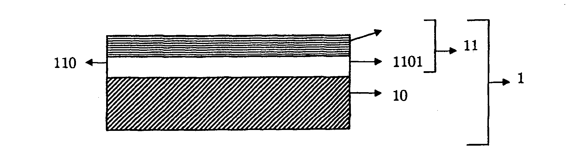
[0244] Table Ia gives in three columns examples of transparent substrates (1) comprising different types of electrodes (number of layers, chemical species of layers and thickness) and the results of measurements of the electrical and optical properties by including these Substrates for organic electroluminescent devices are obtained. The general structure of the electroluminescent device has been described above (page 28, lines 4 to 14). Examples 1R, 2R and 3R are three examples not in accordance with the invention. Example 1R is a transparent substrate comprising ITO electrodes. Example 2R is a transparent substrate comprising an electrode based on a structured low-emission stack comprising an Ag conductive layer. Example 2R is a transparent substrate not optimized for OLEDs because the electrode does not contain a leveling layer (114) and the thickness of the improving coating (110) is not optimized and thus outside the optical thickness range according to the following re...

Embodiment 2 and 3

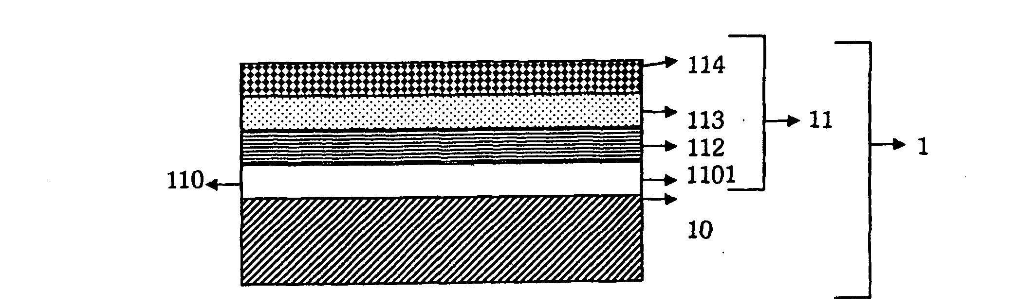
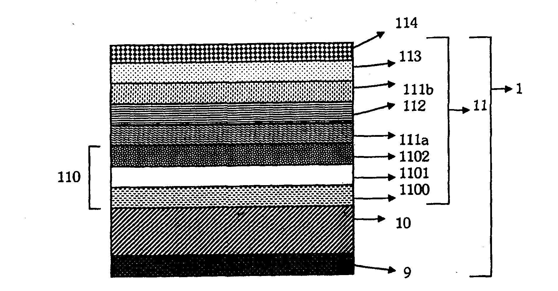
[0312] In Example 1R, the improving coating (114) comprises a barrier layer (1100) combined with a light transmission improving layer (1101) covered by a crystalline layer (1102). In addition, the crystalline layer (1102) and the insertion layer (113) are of the same kind. These layers consist of Zn x sn y o z (where x+y≥3 and z≤6), Zn x sny o z Up to 95% by weight of zinc is contained, the percentages by weight of zinc being expressed relative to the total weight of metal present in the layer. Examples 2 and 3 give examples consistent with the invention. In these embodiments, the improving coating (110) has an optical thickness that conforms to the following relationship:

[0313] T ME =T ME_0 +[B*sin(∏*T D1 / T D1_0 )] / (n 载体 ) 3

[0314] It comprises a barrier layer (1100) combined with an improvement layer (1101) covered by a crystalline layer (1102). Furthermore, the crystalline layer (1102) and the insertion layer (114) are of the same kind. These layers con...

Embodiment 3

[0317] Example 3 illustrates a transparent substrate comprising a thick silver layer which makes it possible to obtain a conductive layer with low resistance.

[0318] A comparison of the properties obtained for devices emitting quasi-white light comprising the transparent substrates of Examples 1R, 2 and 3 shows that:

[0319] The lifetime of the device comprising the substrate according to the invention is longer compared to Example 1R and also compared to a transparent substrate consisting of the same carrier (10) with an ITO electrode located thereon having Equivalent to a geometric thickness of 90 nm, its lifetime was 162 hours (results not shown in Table VII);

[0320] The sheet resistance (Ω / □) of Example 3 with a thick conductive layer is at least half lower than that of Examples 2 and 1R (Ω / □). The possibility of forming larger-sized devices under the circumstances;

[0321] • The optical properties obtained with organic electroluminescent devices comprising example...


PUM

PropertyMeasurementUnit
thicknessaaaaaaaaaa
thicknessaaaaaaaaaa
thicknessaaaaaaaaaa

Abstract

The present invention relates to a transparent substrate (1) for photonic devices, comprising a support (10) and an electrode (11), said electrode (11) comprising a stack comprising a single metallic conduction layer (112) and at least one coating (110) having properties for enhancing the light transmission through said electrode, said coating (110) having a geometric thickness at least greater than 3 nm and at most less than or equal to 200 nm, said coating (110) comprising at least one light-transmission enhancement layer (1101) and being located between the metallic conduction layer (112) and the support (10) on which said electrode (11) is deposited, such that the optical thickness T01 of the coating (110) provided with light-transmission enhancement properties and the geometric thickness TME of the metallic conduction layer (112) are linked through the equation: TME = TME_o + B*sin(pi*TD1 / TD1_0) / n3 support where TME_o, B and TD1_0 are constants with TME_o having a value lying in the range from 10.0 to 25.0 nm, B having a value lying in the range from 10.0 to 16.5 and TD1_0 having a value lying in the range from 23.9 *nD1 nm to 28.3 *nD1 nm where nD1 represents the refractive index of the light-transmission enhancement coating at a wavelength of 550 nm, nsupport represents the refractive index of the support at the 550 nm wavelength.

Description

technical field [0001] The invention belongs to the technical field of photonic devices (dispositif photonique) [0002] The present invention relates to a transparent base material for a photonic device, to a manufacturing method of the base material, and to a manufacturing method of a photonic device comprising the base material. A photonic device refers to any type of device that can emit or collect light. Such devices are, for example, optoelectronic devices, such as organic electroluminescent devices (OLEDs) for short. O organic L right E throwing D evice), or light-harvesting devices such as organic photovoltaic cells, also known as solar cells. In particular, the present invention relates to organic electroluminescent devices (OLED: O organic L right E throwing D evice) transparent substrate. Background technique [0003] Organic electroluminescent devices are produced with good internal light yields. This yield is expressed in internal quantum efficiency (...

Claims


Application Information

Patent Timeline
Patent Type & Authority Applications(China)
IPC IPC(8): H01L51/52H01L51/10C03C17/36
CPCC03C17/38H01L51/102H01L51/52C03C17/3678C03C17/36H01L51/105H01L51/5215H10K10/82H10K10/84H10K50/80H10K50/816
Inventor B·多莫克P·罗奎尼D·德克鲁普特
Owner AGC GLASS EUROPE SA
Why Eureka
Try Eureka