Data reading method and data writing method of memory circuit

A memory circuit and data reading technology, which is applied in the field of data reading of memory circuits and data writing of memory circuits, can solve problems such as increased power consumption and reduced read and write speed, and achieve reduced power consumption and reduced swing , Improve the effect of reading and writing speed

Active Publication Date: 2012-01-25
GIGADEVICE SEMICON (BEIJING) INC
View PDF3 Cites 4 Cited by
  • Summary
  • Abstract
  • Description
  • Claims
  • Application Information

AI Technical Summary

Problems solved by technology

However, with the existing memory cell array, the voltage swing on the bit line must be in the form of a full swing, which will inevitably lead to increased power consumption and reduced read / write speed.

Method used


Image

  • Data reading method and data writing method of memory circuit
  • Data reading method and data writing method of memory circuit
  • Data reading method and data writing method of memory circuit

Examples


Embodiment Construction

[0063] In order to make the above objects, features and advantages of the present invention more comprehensible, the present invention will be further described in detail below in conjunction with the accompanying drawings and specific embodiments.

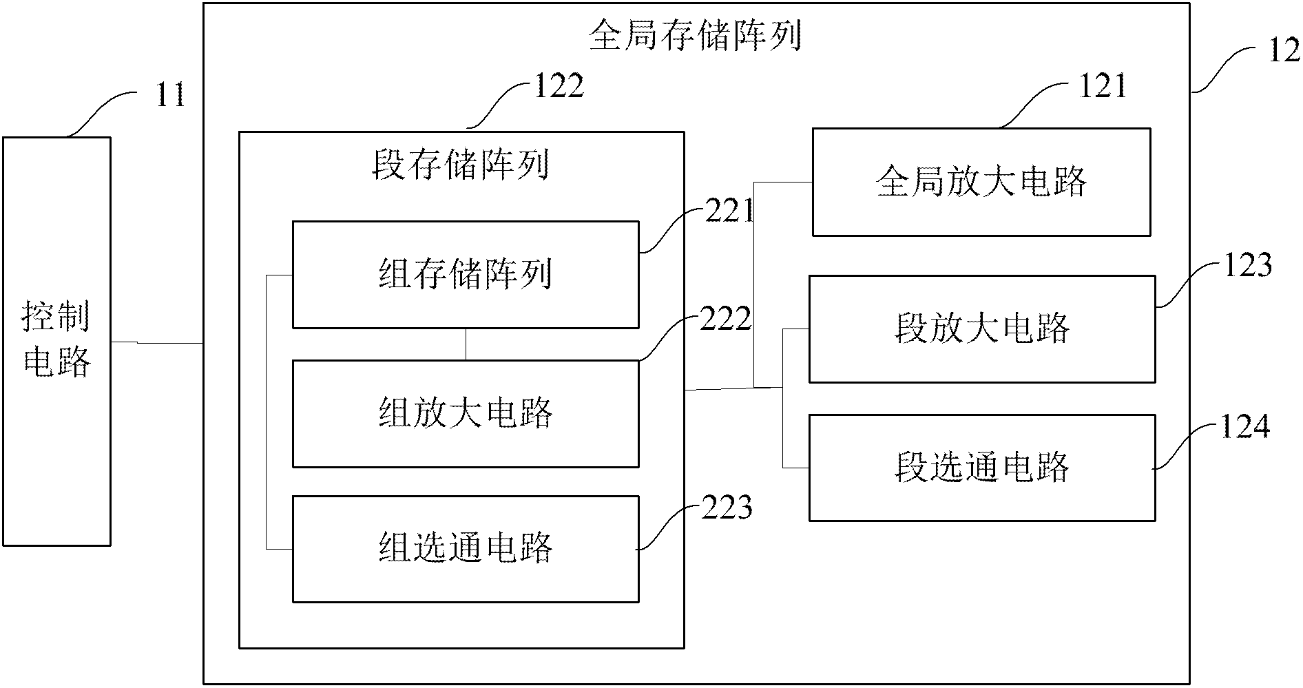
[0064] One of the core concepts of the embodiments of the present invention is to creatively design a global storage array, which is divided into a group storage array and a segment storage array in a multi-level segmented manner, and the segment storage array includes a group storage array Array and group amplification gate circuit; global storage array includes segment memory array, segment amplification gate circuit and global amplification circuit. The global amplifying circuit is connected with the segment amplification gating circuit through the global bit line, the segment amplifying gating circuit is connected with the group amplifying gating circuit through the segment bit line, and the group amplifying gating circuit is c...


PUM


Abstract

The invention provides a data reading method of a memory circuit and a data writing method of the memory circuit. A global memory array is adopted in the memory circuit; a multi-stage and multi-segment mode is adopted by the global memory array; the global memory array is divided into a group memory array and a segment memory array; the segment memory array comprises the group memory array and a group amplifying gate circuit; the global memory array comprises the segment memory array, a segment amplifying gate circuit and a global amplifying circuit; the global amplifying circuit is connectedwith the segment amplifying gate circuit through a global bit line; the segment amplifying gate circuit is connected with the group amplifying gate circuit through a segment bit line; the group amplifying gate circuit is connected with a memory unit in the group array through a group bit line; and through the multi-stage and multi-segment mode, the occupied area of a memory can be small and the swing amplitude of bit line voltage can also be effectively reduced in the layout, so that the aim of reducing power consumption is fulfilled. During data reading and writing operation, the operation is only required to be performed aiming at the currently selected bit line when the global memory array is adopted, so that the reading and writing speed of a memory can also be effectively increased.

Description

technical field [0001] The present invention relates to the technical field of memory, in particular to a data reading method for a memory circuit, and a data writing method for a memory circuit. Background technique [0002] Static RAM memory blocks based on conventional six-transistor (6T) memory cells have been a powerful tool for development in many embedded designs because this memory structure fits well into mainstream CMOS process flows without adding any additional process steps. [0003] In general, basic interleaved coupled latches and active load cells make up a 6T memory cell, which can be used in memory arrays ranging in size from a few bits to several megabits. Carefully designed such memory arrays can meet many different performance requirements, depending on whether the designer chooses a CMOS process optimized for high performance or low power. The access time of an SRAM block produced by a high-performance process can easily be lower than 5ns in a 130nm pr...

Claims


Application Information

Patent Timeline
Patent Type & Authority Applications(China)
IPC IPC(8): G11C7/18
Inventor 刘奎伟
Owner GIGADEVICE SEMICON (BEIJING) INC
Why Eureka
Try Eureka