
Sodium sputtering doping method for large scale cigs based thin film photovoltaic material

A thin-film photovoltaic and sodium-doped technology, which is applied in sputtering coating, metal material coating process, vacuum evaporation coating, etc., can solve the problems that cannot be applied in a wide range of time, difficult to integrate thin films, and poor reliability.

Inactive Publication Date: 2012-02-08
CM MFG
View PDF3 Cites 14 Cited by
  • Summary
  • Abstract
  • Description
  • Claims
  • Application Information

AI Technical Summary

Problems solved by technology

Solar cells made with the aid of thin-film technology have similar limitations, that is, generally poor efficiency
In addition, membranes generally have poor reliability and cannot be applied over a wide range of time periods in conventional environments
Often, thin films are difficult to mechanically integrate with each other
For this reason, the integration of electrode materials and absorber materials formed overlying sodium-containing substrates is also problematic, especially for large-scale manufacturing.

Method used


Image

  • Sodium sputtering doping method for large scale cigs based thin film photovoltaic material
  • Sodium sputtering doping method for large scale cigs based thin film photovoltaic material
  • Sodium sputtering doping method for large scale cigs based thin film photovoltaic material

Examples


Embodiment Construction

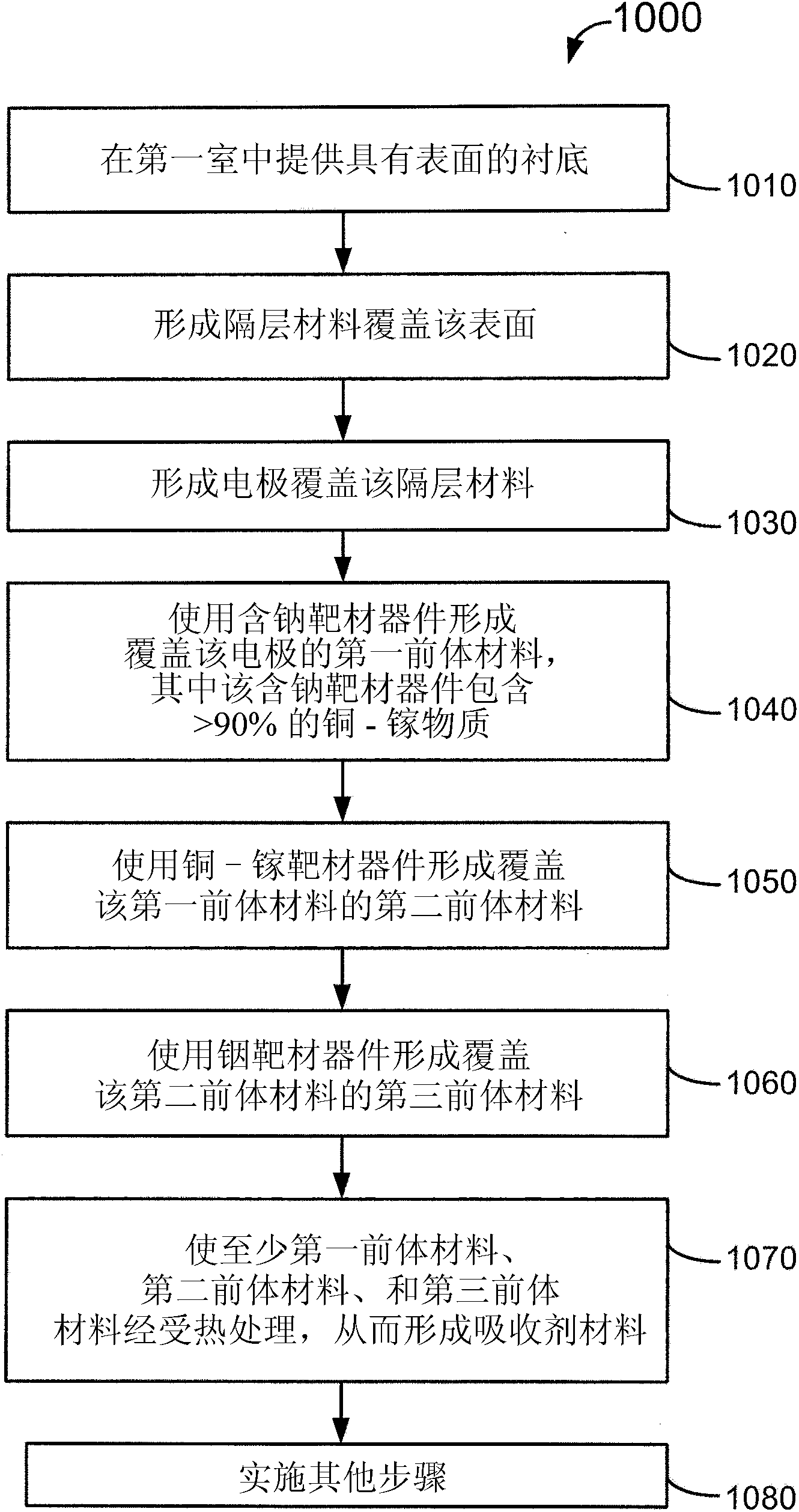
[0014] figure 1 is a flowchart illustrating a method of fabricating a thin film photovoltaic material according to an embodiment of the present invention. The method 1000 includes the following processes:

[0015] 1. Process 1010 for providing a transparent substrate having a surface;

[0016] 2. Process 1020 for forming a barrier material on the surface;

[0017] 3. Process 1030 for forming electrodes;

[0018] 4. Process 1040 for forming a first precursor material overlying the electrode using a sodium-containing target device, wherein the sodium-containing target device comprises >90% copper-gallium species;

[0019] 5. Process 1050 for forming a second precursor material overlying the first precursor material using a copper-gallium target device;

[0020] 6. Process 1060 for forming a third precursor material overlying the second precursor material using an indium target device;

[0021] 7. Process 1070 for subjecting at least a first precursor material, a second prec...


PUM

PropertyMeasurementUnit
thicknessaaaaaaaaaa
thicknessaaaaaaaaaa
thicknessaaaaaaaaaa

Abstract

A method of processing sodium doping for thin-film photovoltaic material includes forming a metallic electrode on a substrate. The invention also discloses a structure used for forming the photovoltaic material. A sputter deposition using a first target device comprising 4-12 wt% of Na 2 SeO 3 and 88-96 wt% of copper-gallium species is used to form a first precursor with a first Cu / Ga composition ratio. A second precursor over the first precursor has copper species and gallium species deposited using a second target device with a second Cu / Ga composition ratio substantially equal to the first Cu / Ga composition ratio. A third precursor comprising indium material overlies the second precursor. The precursor layers are subjected to a thermal reaction with at least selenium species to cause formation of an absorber material comprising sodium species and a copper to indium-gallium atomic ratio of about 0.9.

Description

[0001] References to related applications [0002] This application claims priority to US Provisional Application No. 61 / 367,030, filed July 23, 2010, commonly assigned, and is hereby incorporated by reference in its entirety for all purposes. technical field [0003] The present invention generally relates to thin film photovoltaic (photovoltaic) materials and methods for their production. More specifically, the present invention provides a method and structure for doping sodium in precursors for forming photovoltaic materials. The method includes in-chamber sodium sputter doping for the fabrication of chalcopyrite photovoltaic materials, but it should be recognized that other configurations of the invention are possible. Background technique [0004] Humanity has long been challenged to find ways to harness energy. Energy comes in various forms such as petrochemical, hydroelectric, nuclear, wind, biological resources, sun, trees and coal. Solar technology generally conv...

Claims


Application Information

Patent Timeline
Patent Type & Authority Applications(China)
IPC IPC(8): H01L31/18C23C14/34C23C14/14H01L31/0336
CPCH01L21/02568H01L21/02573H01L21/02614
Inventor 梅·萨奥
Owner CM MFG
Learn More