Light-emitting diode (LED) chip with flip chip structure and manufacturing method thereof

A technology of light-emitting diodes and manufacturing methods, applied in the direction of electrical components, circuits, semiconductor devices, etc., can solve the problems of easily damaged chips and unsatisfactory bonding firmness, so as to improve thermal damage, reduce the influence of electrodes on light, The effect of improving heat dissipation efficiency

Inactive Publication Date: 2014-12-10
EPILIGHT TECH
View PDF6 Cites 0 Cited by
  • Summary
  • Abstract
  • Description
  • Claims
  • Application Information

AI Technical Summary

Problems solved by technology

Among them, most of the existing reverse soldering technology adopts a gold ball bonding method, which is easy to damage the chip, and the bonding firmness is not ideal. Therefore, how to break through the existing bonding technology has become a problem for those skilled in the art. Technical issues to be solved urgently

Method used


Image

  • Light-emitting diode (LED) chip with flip chip structure and manufacturing method thereof
  • Light-emitting diode (LED) chip with flip chip structure and manufacturing method thereof
  • Light-emitting diode (LED) chip with flip chip structure and manufacturing method thereof

Examples


Embodiment Construction

[0022] The fabrication method of the flip-chip light emitting diode chip of the present invention will be described in detail below with reference to the accompanying drawings.

[0023] The manufacturing method of the light-emitting diode chip of flip-chip structure of the present invention comprises the following steps:

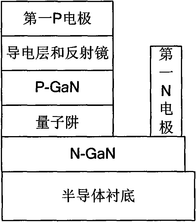
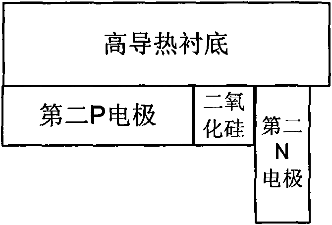
[0024] First, an N-type semiconductor layer, a quantum well layer, and a P-type semiconductor layer are sequentially grown on a semiconductor substrate by epitaxial method, and the first N electrode is made on the N-type semiconductor layer, and the P-type semiconductor layer is successively grown on the P-type semiconductor layer. Make the first P electrode for bonding, thus forming the chip structure to be bonded, such as figure 2 As shown, in order to increase the light extraction rate, a conductive layer and a mirror can be added between the P-type semiconductor layer and the first P-electrode. In this embodiment, the semiconductor substrate may be a s...


PUM


Abstract

The invention provides a light-emitting diode (LED) chip with a flip chip structure and a manufacturing method thereof. The manufacturing method comprises the following steps: firstly, growing out an N-type semiconductor layer, a quantum well layer and a P-type semiconductor layer in sequence on a growth substrate by adopting an epitaxial method; manufacturing a first N electrode on the N-type semiconductor layer and manufacturing a first P electrode for bonding on the P-type semiconductor layer so as to form a chip structure to be bonded; then manufacturing a second N electrode and a second P electrode which respectively correspond to the first N electrode and the first P electrode on another high-heat conduction substrate, and enabling the second N electrode and the second P electrode to be electrically isolated from each other so as to form a substrate structure to be bonded; and then bonding the chip structure with the substrate structure so as to form the light-emitting diode chip. The formed light-emitting diode chip has high light-emitting efficiency and is also capable of improving the temperature damage of power-type LEDs.

Description

technical field [0001] The invention relates to a light-emitting diode chip with a flip-chip structure and a manufacturing method. Background technique [0002] Light-emitting diodes have long service life, short start-up time, firm structure, energy saving, illuminants close to point light sources, wide range of thin lamp materials, no need to apply reflectors, low voltage, no ultraviolet radiation, and are safer to use in public environments. Mercury-free production has many advantages such as environmental protection and energy conservation. Therefore, it is widely used in building exterior lighting, landscape lighting, signage and indicative lighting, indoor space display lighting, entertainment venues and stage lighting, video screens and Industrial design and other fields have a wide range of applications. In particular, high-power light-emitting diodes, because they may realize semiconductor solid-state lighting, have caused a revolution in the history of human light...

Claims


Application Information

Patent Timeline
Patent Type & Authority Patents(China)
IPC IPC(8): H01L33/62H01L33/64
Inventor 张楠齐胜利潘尧波朱广敏叶青郝茂盛
Owner EPILIGHT TECH
Why Eureka
Try Eureka