Digital micro-mirror device and forming method thereof

A digital micromirror device and digital micromirror technology, applied in the field of projectors, can solve the problems of high driving voltage, low yield, high power consumption, etc.

Active Publication Date: 2012-02-15
XIAN YISHEN OPTOELECTRONICS TECH CO LTD
View PDF7 Cites 13 Cited by
  • Summary
  • Abstract
  • Description
  • Claims
  • Application Information

AI Technical Summary

Problems solved by technology

[0005] The problem that the present invention solves is that the digital micromirror device structure of prior art is complicated, and yield rate is low, and driving voltage is high (power consumption is high)

Method used


Image

  • Digital micro-mirror device and forming method thereof
  • Digital micro-mirror device and forming method thereof
  • Digital micro-mirror device and forming method thereof

Examples


Embodiment Construction

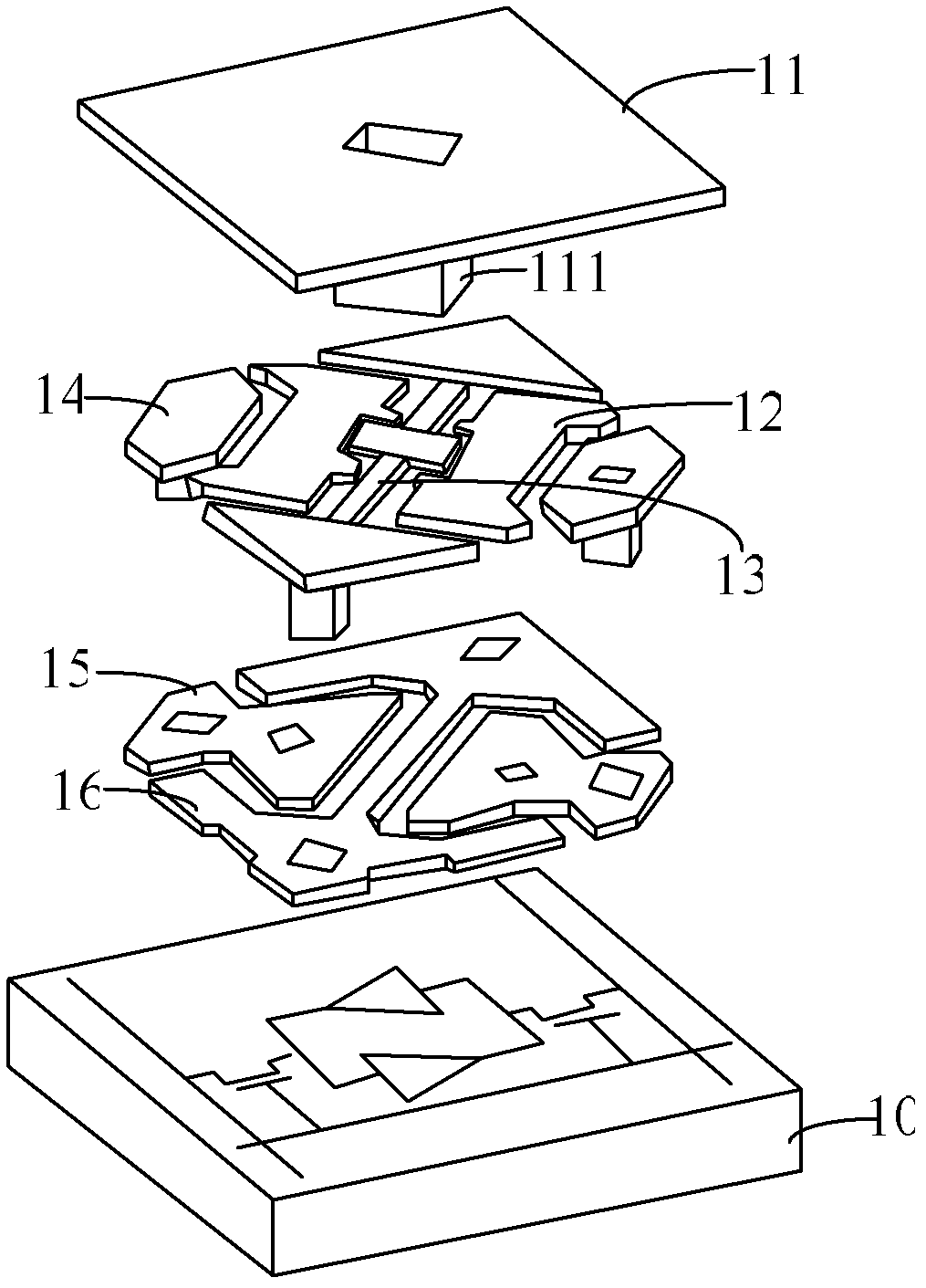
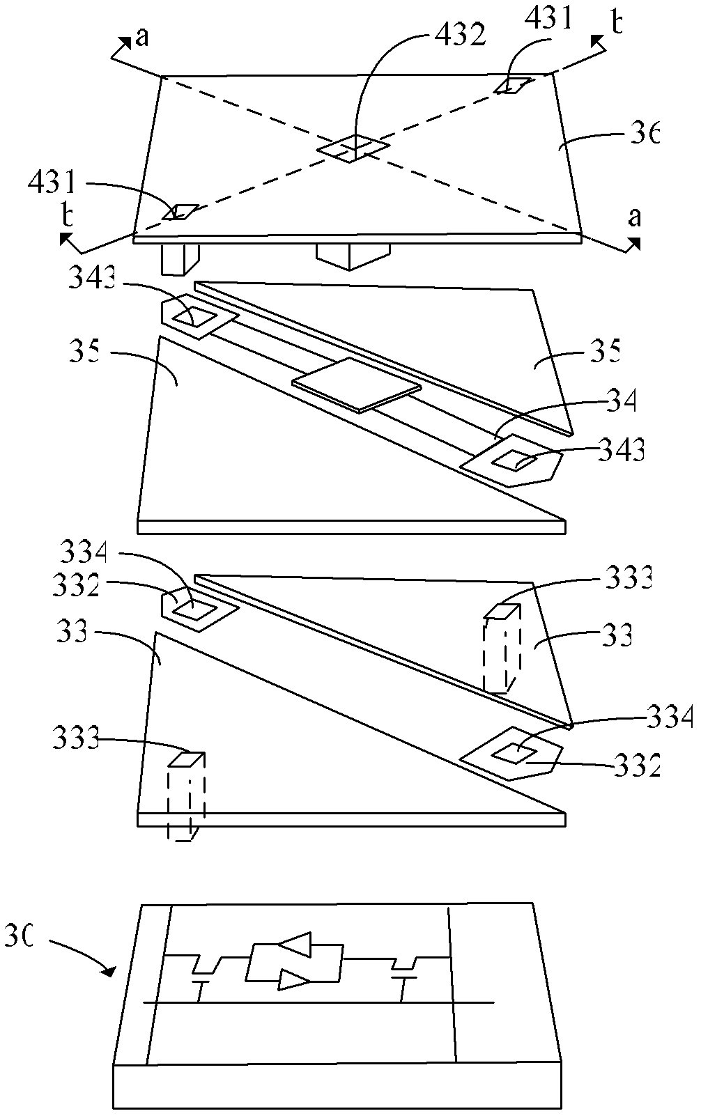
[0094] The digital micromirror device of the invention has a simple structure. Moreover, in a specific embodiment, the hinge includes a conductive layer and a dielectric layer. Due to the existence of the dielectric layer, the strength of the dielectric layer is greater than the strength of the conductive layer. Compared with the hinge that only includes the conductive layer in the prior art, the strength of the hinge is improved. Thereby, the reliability of the hinge can be increased (that is, the number of times the hinge can be turned).

[0095] Further, in the present invention, the first pole plate located above the second pole plate also includes a conductive layer and a dielectric layer, the dielectric layer is close to the second pole plate, and the conductive layer is far away from the second pole plate. In the polar plate, the dielectric layer has compressive stress relative to the conductive layer, and the conductive layer has tensile stress relative to the dielectr...


PUM


Abstract

The invention discloses a digital micro-mirror device and a forming method thereof. The digital micro-mirror device comprises a substrate and a digital micro-mirror array, wherein a micro-mirror device control circuit structure is formed on the substrate; each digital micro-mirror in the digital micro-mirror array comprises a reflecting mirror, two first polar plates, two second polar plates and a hinge; the two second polar plates are positioned on the substrate and are electrically connected with the micro-mirror device control circuit structure; the two first polar plates are positioned above the two second polar plates and respectively opposite to the two second polar plates; the hinge is positioned above the second polar plates; the reflecting mirror is positioned above the first polar plates and is electrically connected with the two first polar plates through first inserting pins; the reflecting mirror is electrically connected with the hinge through a second inserting pin; thehinge is electrically connected with the micro-mirror device control circuit structure; and when voltage difference is reserved between the first polar plates and the second polar plates, the reflecting mirror deflects around the hinge. The digital micro-mirror device has a simple structure and improved reliability of the hinge.

Description

technical field [0001] The invention relates to the technical field of projectors, in particular to a digital micromirror device and a forming method thereof. Background technique [0002] DMD (digital mirror device) digital micromirror device is an integrated MEMS superstructure cell, which is made of CMOS SRAM memory cells. The manufacture of the upper structure of the DMD starts from the complete CMOS memory circuit, and then through the use of the mask layer, the upper structure of the aluminum conductive layer and the hardened photoresist layer (hardened photoresist) are manufactured alternately. The aluminum conductive layer includes the address electrode (address electrode) ), hinge (hinge), yoke (yoke) and mirrors, hardened photoresist layer as a sacrificial layer (sacrificial layer), used to form air gaps (air gaps). The aluminum conductive layer is sputter-deposited and plasma-etched to form address electrodes, hinges, yokes and mirrors; the sacrificial layer is p...

Claims


Application Information

Patent Timeline
Patent Type & Authority Applications(China)
IPC IPC(8): G02B26/08G03F7/00B81B7/02B81C1/00
Inventor 毛剑宏唐德明
Owner XIAN YISHEN OPTOELECTRONICS TECH CO LTD
Why Eureka
Try Eureka