Network structure on non-blocking optical section and communication method thereof

A network structure and non-blocking technology, applied in the field of communication, can solve the problems of low bandwidth of optical routers, many waveguide crossing points, and extended information waiting time, and achieve high-throughput network non-blocking, high utilization of network resources, and information waiting time. The effect of extension

Inactive Publication Date: 2012-02-22
XIDIAN UNIV
View PDF4 Cites 17 Cited by
  • Summary
  • Abstract
  • Description
  • Claims
  • Application Information

AI Technical Summary

Problems solved by technology

The disadvantage of this method is: during the period from when the electrical control network sends the electrical link construction information to reserve the optical link to when the optical information transmission is completed, other processor cores cannot use the reserved optical link even though they are idle. The resource utilization rate of the network is low, and the information waiting delay is long, which aggravates the blocking problem in the network, which further affects the overall performance of the network on the optical chip; the microring resonator and waveguide used in the optical router structure used in the network Many, the structure is complex, and the energy consumed by optical information in the transmission process is relatively large
The disadvantages

Method used


Image

  • Network structure on non-blocking optical section and communication method thereof
  • Network structure on non-blocking optical section and communication method thereof
  • Network structure on non-blocking optical section and communication method thereof

Examples


Embodiment Construction

[0051] The present invention will be further described below in conjunction with the accompanying drawings.

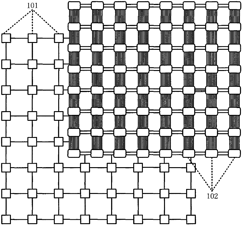
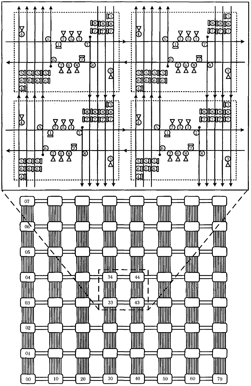
[0052] Refer to attached figure 1 , the non-blocking optical network on chip of the present invention includes 64 processor cores 101 and 64 optical routers 102 . Among them, 64 processor cores 101 are on the electrical layer, which are uniformly and regularly arranged from left to right and from bottom to top to form an 8×8 processor core network, located on the four sides of the 8×8 processor core network. The processor cores at the two corners are respectively connected to the two adjacent processor cores, the other processor cores at the edge of the network are respectively connected to the three adjacent processor cores, and the other processor cores in the processor core network are adjacent to the 64 optical routers 102 are on the optical layer, which are evenly and regularly arranged from left to right and from bottom to top to form an 8×8 optical router netwo...


PUM


Abstract

The invention discloses a network structure on a non-blocking optical section and a communication method thereof, and mainly solves the problems that information waiting time delay in a network is large and the network is blocked on the existing optical section. The network structure comprises 64 processor cores and 64 optical routers, novel non-blocking optical routers are used in the network, and the optical routers are interconnected to form an optical router network in a novel mode. The communication method comprises the following steps: (1) establishing a coordinate system; (2) determining the parameters: a source processor core coordinate, a target processor core coordinate and a wavelength used for sending optical information; (3) sending the optical information; (4) transmitting the optical information in the optical router network; (5) judging whether the optical information reaches the target optical router or not; and (6) receiving the optical information. The invention has the advantages of small communication time delay, not blockage in the network and large throughput, and is suitable for the interconnection and communication between network processor cores on the optical section.

Description

technical field [0001] The invention belongs to the technical field of communication, and further relates to a non-blocking optical network-on-chip network structure and a communication method thereof in the technical field of optical network-on-chip communication. The optical on-chip network network structure of the present invention can be used for optical interconnection between the cores of the network processors on the optical chip; the communication method can be used to set how to communicate between the cores of the network processors on the optical chip. Background technique [0002] In the optical network on chip, because it is difficult to store optical information, the optical-electrical hybrid optical network-on-chip is generally used to realize the communication between processor cores. The non-blocking transmission in the router relieves the blocking of optical information transmission in the network. [0003] A patent application filed by Xi'an University of...

Claims


Application Information

Patent Timeline
IPC IPC(8): H04B10/12H04Q11/00H04L12/56H04B10/27
Inventor 顾华玺白露莹杨银堂岳鹏余晓杉
Owner XIDIAN UNIV
Why Eureka
Try Eureka