High-strength chip packaging structure

A chip packaging structure and high-strength technology, applied in electrical components, electrical solid devices, circuits, etc., can solve problems such as affecting the normal operation of the chip, reducing the service life of the chip, and lacking the stability of the chip packaging structure. Heat dissipation performance, reasonable effect of package structure design

Inactive Publication Date: 2012-03-07
常熟市广大电器有限公司
View PDF4 Cites 0 Cited by
  • Summary
  • Abstract
  • Description
  • Claims
  • Application Information

AI Technical Summary

Problems solved by technology

However, in some heavy-duty or high-speed mechanical equipment, the chip is often subjected to alternating stress or impact load, and the chip packaging structure lacks stability, which affects the normal operation of the chip and reduces the service life of the chip

Method used


Image

  • High-strength chip packaging structure
  • High-strength chip packaging structure

Examples


Embodiment Construction

[0017] The preferred embodiments of the present invention will be described in detail below in conjunction with the accompanying drawings, so that the advantages and features of the present invention can be more easily understood by those skilled in the art, so as to define the protection scope of the present invention more clearly.

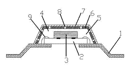
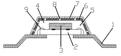
[0018] figure 1 It is a structural schematic diagram of a high-strength chip packaging structure in an embodiment of the present invention; the high-strength chip packaging structure mainly includes metal pins 1, a substrate 2, a chip 3 and a package body 4, and it is characterized in that the package body 4 adopts a multilayer Structural design, from the inside to the outside is composed of a sealant layer 5, a metal layer 6 and a heat dissipation layer 7, the metal layer 6 adopts a metal spraying process, and is formed on the surface of the sealant layer 5. The heat dissipation layer 7 is pasted On the outside of the metal layer 6, it plays the...


PUM


Abstract

The invention discloses a high-strength chip packaging structure, which mainly comprises a metal pin, a substrate, a chip and a package body and is characterized in that the package body adopts a multi-layer structure which comprises a glue sealing layer, a metal layer and a heat dissipation layer from inside to outside, wherein a metal spraying process is used for the metal layer which is formed on the surface of the glue sealing layer; and the heat dissipation layer is adhered to the outside of the metal layer, thus playing heat dissipation and protection roles. The high-strength chip packaging structure is reasonable in design and easy to implement; the package body in the packaging structure adopts the multi-layer structure, thus playing a multiple protection role in the chip, and effectively improving the strength and toughness of the packaging structure; and in addition, the packaging structure has good heat dissipation performance, ensures the high-efficiency running of the chip, and effectively improves the service life of the chip.

Description

technical field [0001] The invention relates to a chip packaging structure, in particular to a chip packaging structure with high strength, excellent heat dissipation performance and simple process implementation, belonging to the technical field of chip packaging. Background technique [0002] In the manufacture of integrated circuits, chips are obtained through the steps of wafer fabrication, forming integrated circuits, and cutting wafers. After the integrated circuit of the wafer is fabricated, the chip formed by dicing the wafer can be electrically connected to the carrier outwardly; wherein, the carrier can be a lead frame or a substrate, and the chip can be wire bonded or covered. The method of crystal bonding is electrically connected to the carrier. If the chip and the carrier are electrically connected by wire bonding, then enter into the manufacturing step of filling the encapsulant to form the chip package. Chip packaging technology is a process technology that...

Claims


Application Information

Patent Timeline
Patent Type & Authority Applications(China)
IPC IPC(8): H01L23/31H01L23/36
CPCH01L2224/48091H01L2224/48247
Inventor 徐子旸
Owner 常熟市广大电器有限公司
Why Eureka
Try Eureka