Linear voltage regulator and current sensing circuit thereof
A linear voltage regulator and current sensing technology, applied in the direction of measuring current/voltage, instruments, measuring devices, etc., can solve the problems of large frequency variation of non-dominant poles and insufficient phase margins
- Summary
- Abstract
- Description
- Claims
- Application Information
AI Technical Summary
Problems solved by technology
Method used
Image
Examples
no. 1 example
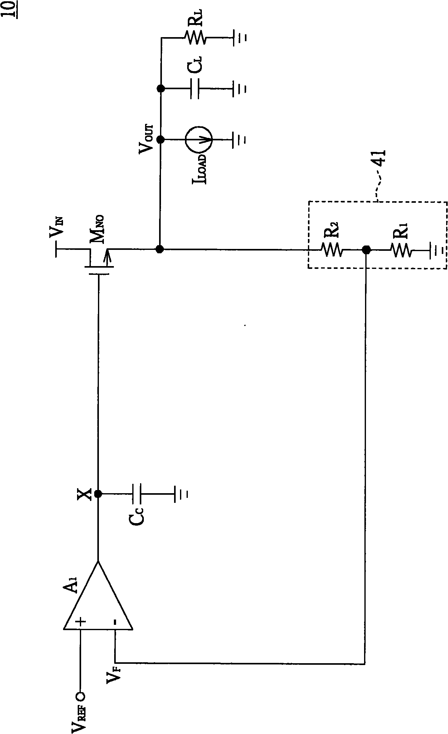
[0054] Please refer to Figure 4 , Figure 4 Shown is a schematic diagram of the architecture of a linear regulator. The linear regulator 40 is, for example, a high drop out (High Drop Out, HDO) linear regulator. The linear regulator 40 includes a pass transistor M NO , compensation capacitor C C , feedback circuit 41, error amplifier A 1 , a variable resistor 42 and a current sensing circuit 43 . For the sake of illustration, Figure 4 The pass transistor M shown NO Taking N-type metal-oxide-semiconductor (Metal-Oxide-Semiconductor, MOS) transistor as an example, the type of transfer transistor is not limited to this, and P-type metal-oxide-semiconductor transistors, NPN bicarrier junction transistors ( BipolarJunction Transistor, BJT) or PNP bipolar junction transistor.
[0055] pass transistor M NO The first terminal receives the input voltage V IN , the transfer transistor M NO The second terminal outputs the output voltage V OUT . pass transistor M NO The fi...
no. 2 example
[0064] Please refer to Figure 6 , Figure 6 Shown is a circuit diagram of the linear regulator of the second embodiment. In the second embodiment, the linear voltage regulator 40, the variable resistor 42 and the current sensing circuit 43 are respectively the linear voltage regulator 40(2), the variable resistor 42(2) and the current sensing circuit 43(1) As an example. The main difference between the second embodiment and the first embodiment lies in the variable resistor 42(2). The variable resistor 42(2) except the aforementioned transistor M N2 additionally, including transistor M N3 . Transistor M N3 The first end and the second end of the transistor M are such as the drain and the source respectively, and the transistor M N3 The control terminal of is, for example, the gate. Transistor M N3 The first terminal of is coupled to the transistor M N3 The control terminal and the transistor M N3 The second terminal is coupled to the compensation capacitor C C and...
no. 3 example
[0067] Please refer to Figure 7 , Figure 7 Shown is a circuit diagram of the linear regulator of the third embodiment. In the third embodiment, the linear voltage regulator 40, the variable resistor 42 and the current sensing circuit 43 are respectively the linear voltage regulator 40(3), the variable resistor 42(3) and the current sensing circuit 43(2) As an example. The main difference between the third embodiment and the second embodiment lies in the variable resistor 42(3) and the current sensing circuit 43(2). The current sensing circuit 43(2) further includes a transistor M N2 , transistor M N2 It is coupled between the variable resistor 42(3) and the ground. Transistor M N2 The control terminal is coupled to the operational amplifier A 2 The output terminal, and the transistor M N2 Controlled by the op amp A 2 . Variable resistor 42(3) includes only transistor M N3 . Transistor M N3 The first end and the second end of the transistor M are such as the drai...
PUM
 Abstract
Description
Claims
Application Information


