Manufacturing method of shallow trench isolation structure

A technology for shallow trench isolation and manufacturing methods, which is applied in the field of shallow trench isolation structure fabrication, and can solve problems affecting the isolation effect of semiconductor devices, semiconductor device failure, and voids

Inactive Publication Date: 2012-03-14
SEMICON MFG INT (SHANGHAI) CORP +1
View PDF3 Cites 6 Cited by
  • Summary
  • Abstract
  • Description
  • Claims
  • Application Information

AI Technical Summary

Problems solved by technology

However, there is also a defect in this method: in the process of depositing the oxide layer 40 in step 103 and filling the STI trench 20, the blocking nitride layer 102 and the isolation oxide pad 101 are etched back to cause the blocking nitride layer 102 and There is a step difference between the isolation oxide pad 101 and the underlying substrate 10, so there will be a filling gap in the middle of the STI groove 20, which will cause a gap to appear in the final formed STI, which will affect the isolation effect of the semiconductor device and seriously cause the semiconductor device to fail.

Method used


Image

  • Manufacturing method of shallow trench isolation structure
  • Manufacturing method of shallow trench isolation structure
  • Manufacturing method of shallow trench isolation structure

Examples


Embodiment Construction

[0035] In order to make the object, technical solution and advantages of the present invention clearer, the present invention will be further described in detail below with reference to the accompanying drawings and examples.

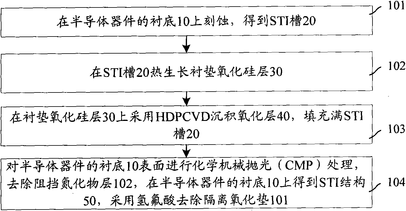
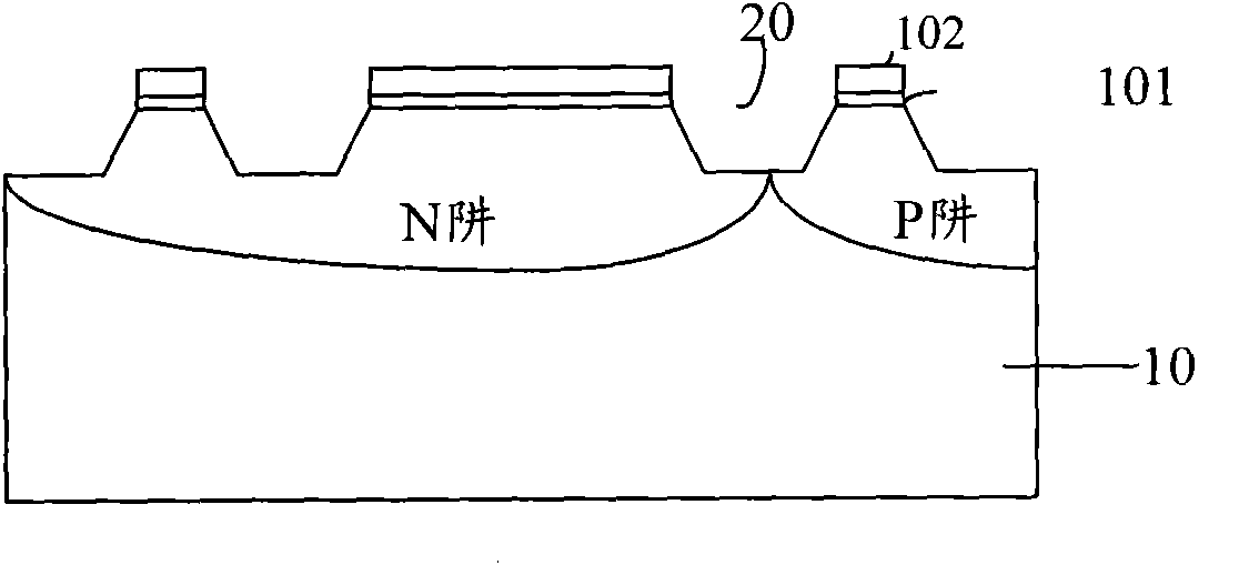
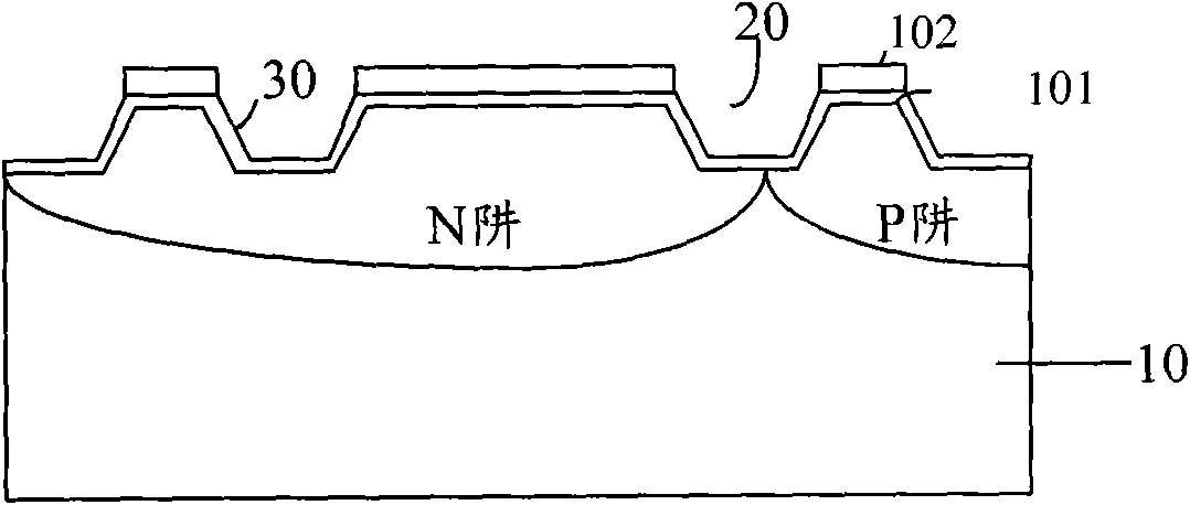
[0036] In order to ensure that the fabricated STI structure has a conforming morphology, that is, there are no gaps in the middle, the present invention does not adopt the step-back engraving of the barrier nitride layer 102 and the isolation oxide pad 101 in the prior art during the fabrication of the STI structure. Eclipse step. In order to ensure that the manufactured STI structure avoids poor defects, it cannot be filled by the gate oxide layer in the subsequent gate manufacturing process, and the material of the STI structure is changed, that is, after the formation of the STI groove, the oxygen-nitride-oxygen structure is used. Fill the STI groove, then dry etch the upper silicon dioxide layer in the oxynitride structure to the height of the STI s...


PUM

PropertyMeasurementUnit
thicknessaaaaaaaaaa

Abstract

The invention discloses a manufacturing method of a shallow trench isolation structure, which comprises the steps that after an isolation oxide pad and a blocking silicon nitride layer are sequentially deposited on a silicon substrate of a semi-conductor device, a shallow trench isolation tank is formed on the silicon substrate of the semi-conductor device through a lithography process and an etching process; a substrate silicon oxide layer is grown on the surface of the shallow trench isolation tank; a silicon nitride layer is deposited on the substrate silicon oxide layer; a silicon dioxide layer is deposited on the surface of the silicon nitride layer, and the shallow trench isolation tank is fully filled; and after the height of the silicon dioxide layer which is etched through a dry process reaches the height of the shallow trench isolation structure and the silicon nitride layer and the substrate silicon oxide layer on the blocking silicon nitride layer are sequentially removed, the surface of the silicon substrate is polished through a chemical mechanical process, the shallow trench isolation structure is obtained and the isolation oxide pad is removed. The shallow trench isolation (STI) structure which is manufactured through the method not only avoids the phenomenon of defects, but also avoids a gap in the STI structure.

Description

technical field [0001] The invention relates to the technical field of semiconductors, in particular to a method for manufacturing a shallow trench isolation (STI) structure. Background technique [0002] In the manufacturing process of the semiconductor device, the manufacturing of the STI structure is included. The fabrication of the STI structure is the isolation region between the active regions fabricated on the substrate of the semiconductor device. The manufacturing method of the STI structure is mainly divided into three steps: etching of the STI groove, filling of the STI material, and planarization of the STI structure. The existing method of manufacturing the STI structure will be described in detail below. [0003] figure 1 A flow chart of a method for making a shallow trench isolation structure provided for the prior art, combined with Figure 2a ~ Figure 2d The schematic diagram of the shallow trench isolation structure shown in the figure is illustrated, an...

Claims


Application Information

Patent Timeline
Patent Type & Authority Applications(China)
IPC IPC(8): H01L21/762
Inventor 宁振佳
Owner SEMICON MFG INT (SHANGHAI) CORP
Why Eureka
Try Eureka