

OLED (Organic light-emitting diode) lighting substrate and manufacture method thereof
A manufacturing method and substrate technology, applied in semiconductor/solid-state device manufacturing, electrical components, electrical solid-state devices, etc., can solve problems such as electrode burnout, cathode-anode short-circuit light emission, unevenness, etc., to reduce the probability of short-circuit The effect of burning out and weakening the current gathering effect
- Summary
- Abstract
- Description
- Claims
- Application Information
AI Technical Summary
Problems solved by technology
Method used
Image

Examples
Embodiment Construction
[0024] The present invention will be further described below in conjunction with the accompanying drawings and embodiments.
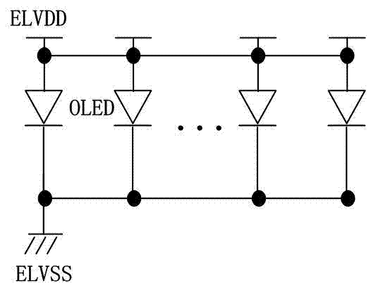
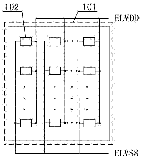
[0025] figure 2 It is a structural schematic diagram of the resistance-driven organic light-emitting display device of the present invention; image 3 It is a schematic diagram of a pixel equivalent circuit of the resistance-driven organic light-emitting display device of the present invention.
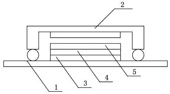
[0026] Please refer to Figure 1~ image 3 , The OLED lighting substrate of the present invention comprises a substrate 1, on which an anode 3, an organic functional layer 4 and a cathode 5 are sequentially arranged, wherein a resistance layer is arranged between the substrate 1 and the anode 3, and the resistance layer Divided into multiple block resistors, the anode 3 is divided into multiple sub-anodes, each sub-anode is connected in series with a block resistor, and the multiple block resistors are connected together through interconnecting wires.
[002...
PUM
 Abstract
Description
Claims
Application Information