Layout structure of power metal oxide semi-field effect transistor (power MOSFET)

A metal-oxygen semi-field, layout structure technology, applied in semiconductor devices, electrical components, circuits, etc., can solve the problems of poor transistor layout integration, large layout area, and increased manufacturing costs.

Inactive Publication Date: 2012-03-21
FORTUNE SEMICON
View PDF5 Cites 0 Cited by
  • Summary
  • Abstract
  • Description
  • Claims
  • Application Information

AI Technical Summary

Problems solved by technology

However, the layout area required by this layout method is relatively large, resulting in poor integration of the traditional power MOSFET layout and increased manufacturing costs.

Method used


Image

  • Layout structure of power metal oxide semi-field effect transistor (power MOSFET)
  • Layout structure of power metal oxide semi-field effect transistor (power MOSFET)
  • Layout structure of power metal oxide semi-field effect transistor (power MOSFET)

Examples


Embodiment Construction

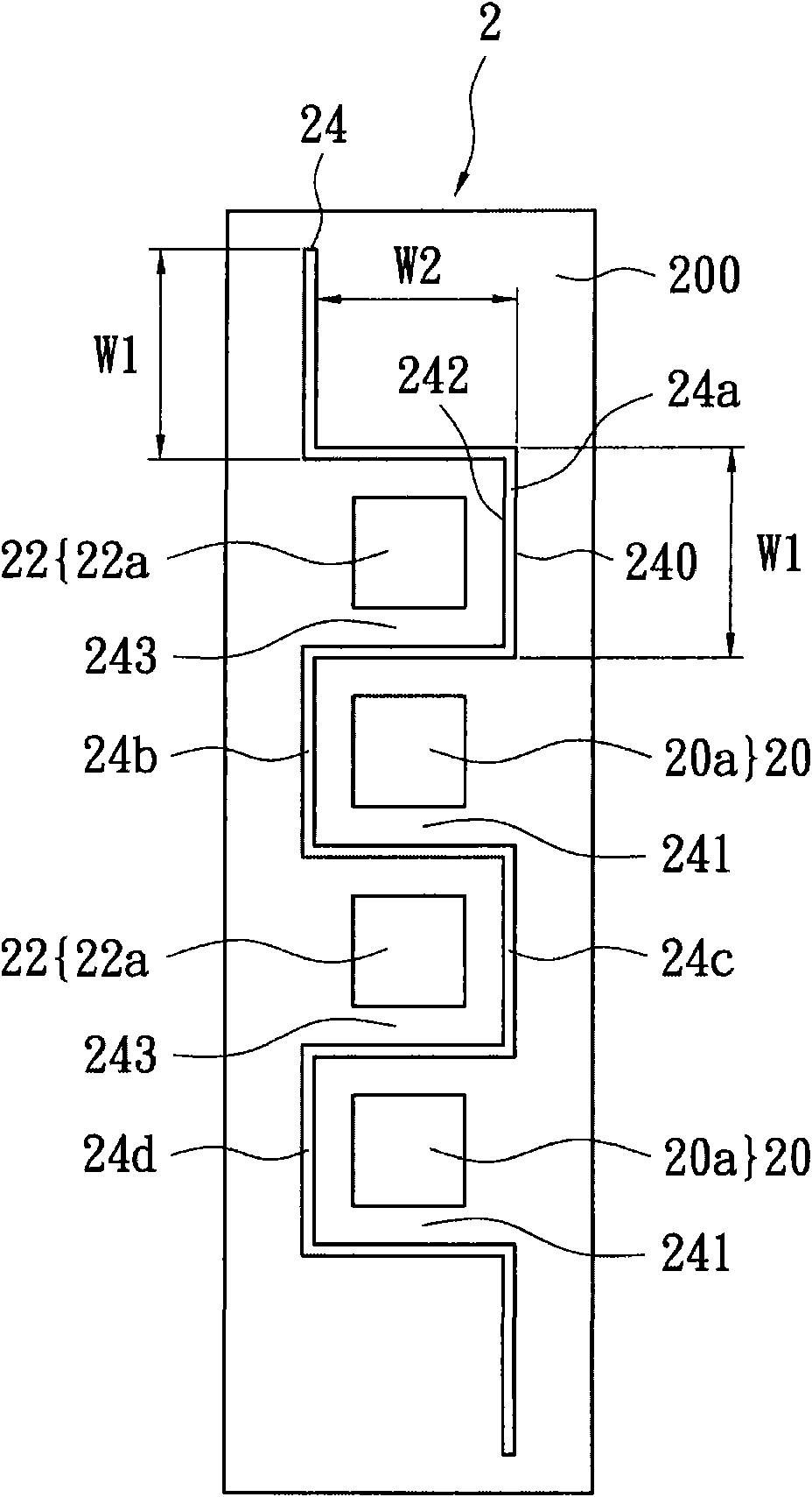
[0045] In order to effectively solve the problem of increased manufacturing cost caused by relatively large layout area required for traditional power metal oxide semiconductor field effect transistors in large sizes. The present invention provides a layout structure of a power metal-oxide-semiconductor field-effect transistor, in which the grid structure in a power metal-oxide-semiconductor field-effect transistor is laid out in a meandering form (such as a zigzag, an S-shape, a square waveform, etc.) on the substrate. With the aid of a snake-like layout structure, the power MOS field effect transistor of the present invention can increase the channel effective width (Channel Width) under the same layout area compared with conventional power MOS field effect transistors.

[0046] According to the formula (1), the output current I of the power MOSFET D It is directly proportional to the effective channel width W, therefore, under the same layout area, the output current capab...


PUM


Abstract

The invention discloses a layout structure of a power metal oxide semi-field effect transistor (power MOSFET). The layout structure comprises a first sinuous grid structure, a first contact structure and a second contact structure, wherein the first sinuous grid structure is arranged in a substrate and provided with a first edge and a second edge; the first contact structure is arranged in the substrate and positioned at the first edge of the first sinuous grid structure; and the second contact structure is arranged in the substrate and positioned at the second edge of the first sinuous grid structure.

Description

technical field [0001] A layout structure of a power metal oxide field effect transistor (Power MOSFET), especially a layout structure that can increase the channel width of a power transistor in the same area by means of a layout of a gate structure. Background technique [0002] When designing voltage conversion circuits such as power converters (DC-DC), low dropout (LDO) regulators, switching regulators (switching regulators) and chargers (chargers), the power metal oxide semiconductors used Considering the characteristics of dropout voltage (dropout voltage), drain-to-source resistance (Rdson) and output current (output current), a field effect transistor (Power MOSFET) needs to be realized with a larger size. [0003] refer to Figure 1A , Figure 1A It is a schematic diagram of the layout of a conventional power MOSFET. The power MOSFET 1 has a strip-shaped gate structure 14 located on a substrate 100 . In the substrate 100 on both sides of the gate structure 14 , on...

Claims


Application Information

Patent Timeline
Patent Type & Authority Applications(China)
IPC IPC(8): H01L29/78H01L29/423
CPCH01L29/4238
Inventor 陈国强陈宴毅周建平
Owner FORTUNE SEMICON
Why Eureka
Try Eureka