Integrated thin-film photovoltaic device and manufacturing method thereof

A technology for optoelectronic components and manufacturing methods, which is applied in the fields of electrical components, photovoltaic power generation, and final product manufacturing, and can solve problems such as shortage of raw materials and rising prices.

Inactive Publication Date: 2012-03-21
韩国铁钢株式会社 +1
View PDF5 Cites 3 Cited by
  • Summary
  • Abstract
  • Description
  • Claims
  • Application Information

AI Technical Summary

Problems solved by technology

However, due to the shortage of raw materials due to the sudden increase in demand for bulk silicon photovoltaic devices, prices are on the rise

Method used


Image

  • Integrated thin-film photovoltaic device and manufacturing method thereof
  • Integrated thin-film photovoltaic device and manufacturing method thereof
  • Integrated thin-film photovoltaic device and manufacturing method thereof

Examples


no. 1 example

[0045] Figure 2a ~ Figure 2g A method of manufacturing an integrated thin film photovoltaic element according to a first embodiment of the present invention is shown.

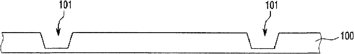
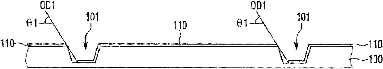
[0046] Such as Figure 2aAs shown, a substrate 100 formed with grooves 101 is prepared. The substrate 100 is preferably made of a transparent insulating material or an opaque insulating material or a transparent conductive material or an opaque conductive material with excellent light transmittance. For example, when a transparent insulating material is used, the substrate 100 may be one of a glass substrate such as soda lime glass or tempered glass, a transparent plastic substrate, or a nanocomposite substrate. A nanocomposite material is a material in which nanocrystalline grains are dispersed in a disperse medium (matrix, continuous phase) in the form of a disperse phase. The dispersion medium can be organic solvents, plastics, metals or ceramics, and the nanocrystalline grains can be plastics, metals or...

no. 2 example

[0081] Figure 3a ~ Figure 3f A method of manufacturing a see-through type integrated thin film photovoltaic element according to an embodiment of the present invention is shown.

[0082] Such as Figure 3a As shown, a substrate 200 in which grooves 201, 203, 205 and holes 202, 204 are formed is prepared.

[0083] The holes 202 , 204 are located between adjacent grooves 201 , 203 , 205 . A series connection is formed between adjacent unit cells in the grooves 201, 203, 205, and the holes 202, 204 are for light transmission. The grooves 201 , 203 , 205 and the holes 202 , 204 can be formed by the same method, and the method of forming the grooves 201 , 203 , 205 and the holes 202 , 204 has been described in the first embodiment, so it is omitted. At this time, the grooves 201, 203, 205 and the holes 202, 204 may be formed simultaneously.

[0084] The ratio of depth d1 to width w1 or diameter w1 of holes 202 , 204 may be greater than the ratio of depth d2 to width w2 of groo...

no. 3 example

[0095] Figure 4a ~ Figure 4e A method of manufacturing an integrated thin film photovoltaic element according to a third embodiment of the present invention is shown.

[0096] Such as Figure 4a As shown, a substrate 300 is prepared in which grooves 301 are formed such that both side surfaces are inclined at an angle α in the same direction at regular intervals.

[0097] Such as Figure 4b As shown, the first pure silicon is discharged in the direction perpendicular to the substrate in the first impurity atmosphere or together with the first impurity or the first extrinsic silicon substance is discharged in the vertical direction to the substrate, and the first extrinsic silicon is discharged in the groove A part of the bottom surface and a side surface of 301 are crystallized during or after deposition on the region between adjacent grooves 301 . Thus, the first extrinsic polysilicon layer 310 is formed. In the third embodiment, since the groove 301 is inclined, the firs...


PUM


Abstract

Disclosed is an integrated thin film photovoltaic device. The integrated thin film photovoltaic device includes: a substrate including trenches formed therein; a first semiconductor material layer formed on the substrate from a first basic line within each of the trenches through one side of each of the trenches to the projected surface of the substrate, which is adjacent to the one side; a second semiconductor material layer formed on a resultant substrate from a second basic line on the first semiconductor material layer within each of the trenches through the other side of each of the trenches to the projected surface of the resultant substrate, which is adjacent to the other side, so that a portion of the first semiconductor material layer and a portion of the second semiconductor material layer are overlapped with each other within each of the trenches.

Description

technical field [0001] The invention relates to an integrated thin film photoelectric element and a manufacturing method thereof. Background technique [0002] Photoelectric elements are devices that directly convert solar energy into electrical energy, and are roughly classified into silicon, compound, and organic types according to the materials used. [0003] According to the phase of semiconductor, silicon optoelectronic elements are subdivided into single crystal silicon (singlecrystalline silicon; c-Si) optoelectronic elements, polycrystalline silicon (polycrystalline silicon; poly-Si) optoelectronic elements, amorphous silicon (amorphous silicon; a-Si:H) optoelectronic elements . [0004] In addition, according to the thickness of the semiconductor, photovoltaic elements are classified into bulk photovoltaic elements and thinfilm photovoltaic elements. Thinfilm photovoltaic elements include a photoelectric conversion material layer with a thickness of several tens of...

Claims


Application Information

Patent Timeline
Patent Type & Authority Applications(China)
IPC IPC(8): H01L31/18H01L27/142H01L31/05H01L31/046H01L31/0465H01L31/0468H01L31/068
CPCY02E10/546H01L31/072H01L27/1426H01L31/03682Y02E10/50H01L31/03921H01L31/1872H01L27/1423H01L31/0504H01L31/05H01L31/046H01L31/0465H01L31/0468Y02E10/547Y02P70/50
Inventor 林宏树全振完
Owner 韩国铁钢株式会社
Why Eureka
Try Eureka