Supercharge Your Innovation With Domain-Expert AI Agents!

Integrated light-emitting diode (LED) light source and manufacturing method thereof

A technology of LED light source and manufacturing method, which is applied in the direction of electrical components, electric solid devices, circuits, etc., can solve the problems of large internal stress between the solder feet of electronic components and the substrate, affecting the connection reliability of electronic components, and affecting the life of LED lamps, etc., to achieve Ensures reliability, protects gold wires, and prolongs service life

Inactive Publication Date: 2012-03-21
杨罡
View PDF8 Cites 3 Cited by
  • Summary
  • Abstract
  • Description
  • Claims
  • Application Information

AI Technical Summary

Problems solved by technology

The integrated light source made by this scheme needs to use the reflow soldering process, and the thermal expansion coefficient between the circuit board and the chip is different. After the circuit board passed the reflow soldering process is cooled, the internal stress of the solder feet of the electronic components and the substrate will be too large. It affects the reliability of the connection of electronic components. Once the pins are desoldered, it will cause the LED lamp to fail and affect the life of the LED lamp.
In addition, the heat of electronic components can only be transferred to the circuit board through the pins. There are multiple layers of heat resistance between the chip inside the electronic component and the circuit board, which affects the life of the light source.

Method used


Image

  • Integrated light-emitting diode (LED) light source and manufacturing method thereof
  • Integrated light-emitting diode (LED) light source and manufacturing method thereof
  • Integrated light-emitting diode (LED) light source and manufacturing method thereof

Examples


Embodiment Construction

[0033] The first embodiment of the integrated LED light source and its manufacturing method:

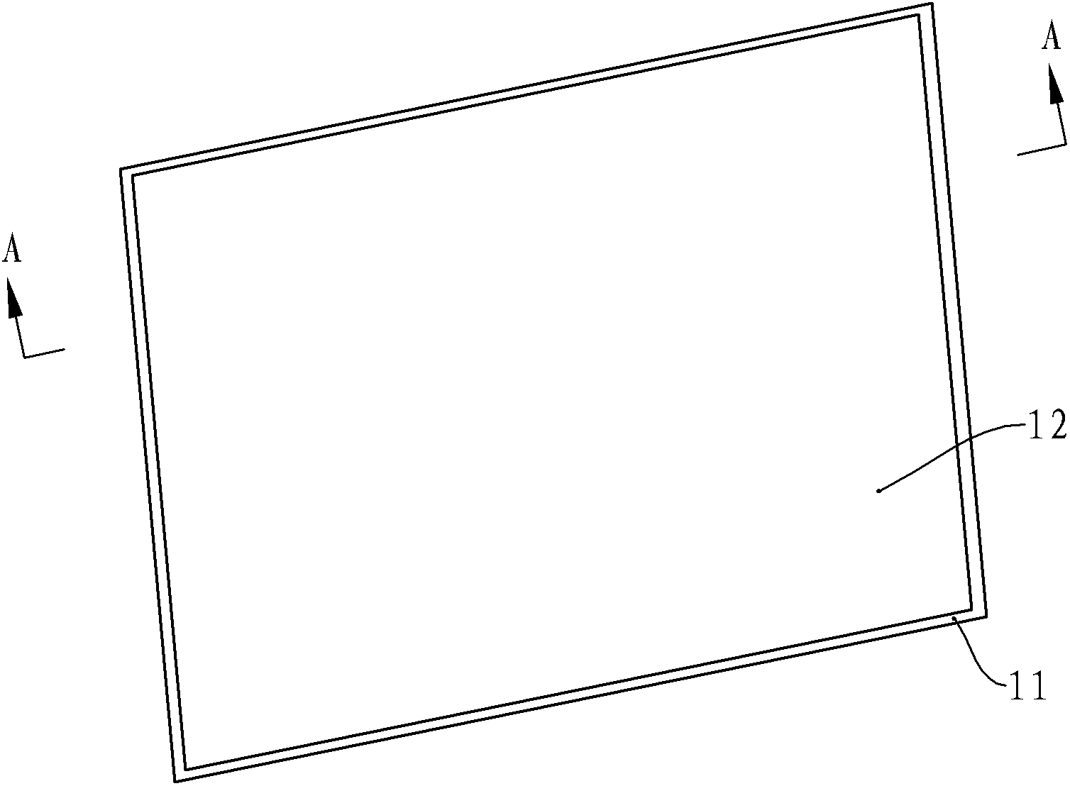
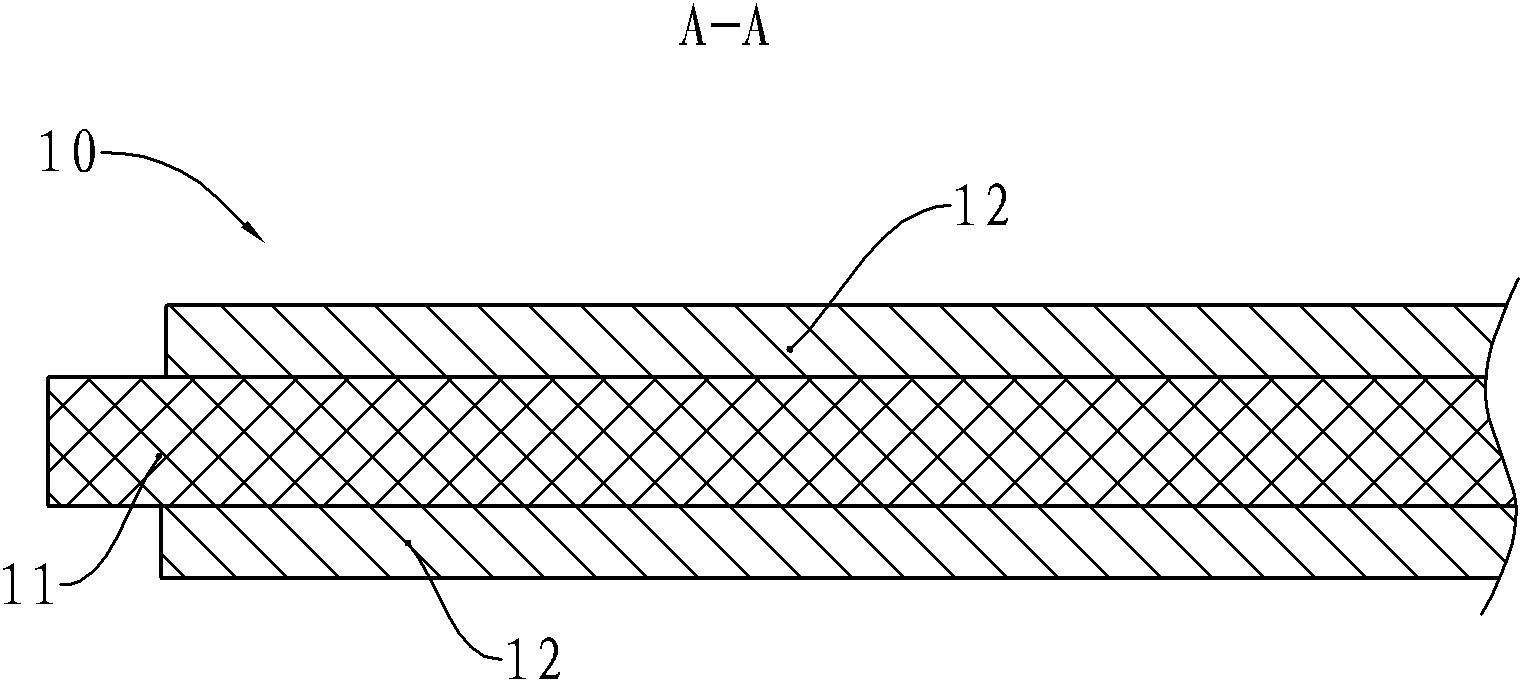
[0034] see figure 1 and figure 2 , the substrate 10 of this embodiment is a double-sided copper-clad ceramic board (DBC, Direct Bonded Copper), the double-sided copper-clad ceramic board has an interlayer 11 made of a ceramic material with high thermal conductivity, and both sides of the interlayer 11 are coated with copper Foil 12 , copper foil 12 almost covers the surface of interlayer 11 .

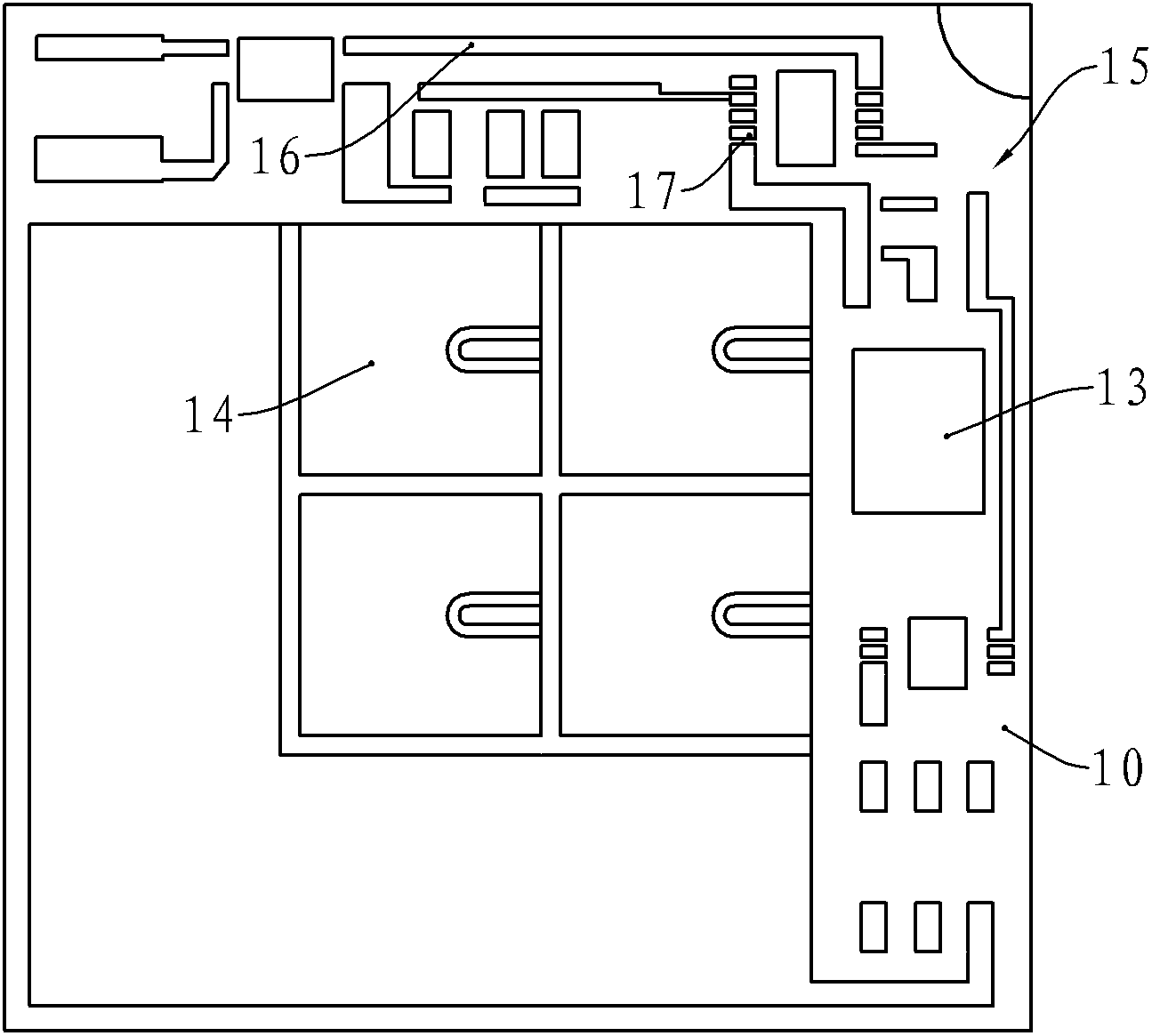
[0035] Such as image 3 As shown, when manufacturing the LED light source, first, the copper foil on the front side of the substrate 10 is etched to form pads 13, 14 and lines 15, wherein the lines 15 include line areas 16 and pin areas 17, and the pads 13 are used for mounting The heat sink pad of the peripheral chip, the pad 14 is a heat sink pad for attaching the LED chip. The lead area 17 is an area for soldering gold wires, and the line area 16 is used for connecting multiple lead ar...


PUM


Abstract

The invention provides an integrated light-emitting diode (LED) light source and a manufacturing method thereof. The integrated LED light source comprises a substrate. One or more LED chips are arranged on the substrate. A peripheral chip is integrated on the substrate. The substrate is a direct bonded copper, and is provided with an interlayer made from a ceramic material. The two sides of the interlayer are clad with a copper foil respectively. The copper foil on one side of the interlayer is etched to form heat sink soldering-pans and a line, and the line is provided with a line region andpin regions. The LED chip and the peripheral chip are arranged on the soldering-pans. Gold wires are connected between the electrodes of the peripheral chip and the pin regions. A first adhesive layer is covered on the line region and the peripheral chip. A second adhesive layer formed after the first adhesive layer is covered on the first adhesive layer. A third adhesive layer formed after the first adhesive layer is covered on the LED chip. The invention also provides the manufacturing method for the integrated LED light source. By the integrated LED light source and the manufacturing method thereof, the line and the gold wires can be effectively prevented from being damaged; and the integrated LED light source can be directly connected with commercial power for use.

Description

technical field [0001] The present invention relates to an integrated LED light source for lighting, in particular to an integrated LED light source with high reliability and long service life based on a double-sided copper-clad ceramic substrate and a manufacturing method for the integrated LED light source. Background technique [0002] As a new type of lighting source, LED light source has the advantages of energy saving, environmental protection, long service life and low consumption. It has been widely used in home lighting, commercial lighting, road lighting, industrial and mining lighting and other occasions. [0003] Most of the existing LEDs are packaged in a single high-power way, and use a metal aluminum substrate as a heat conduction and heat dissipation material. One or more packaged SMD LED light sources are arranged on the substrate. Since the existing LED light source is to connect the packaged single LED to the substrate using the surface mount process or he...

Claims


Application Information

Patent Timeline
IPC IPC(8): H01L33/48H01L33/64H01L33/62H01L33/50H01L25/075H01L33/00
Inventor 杨罡容学宇
Owner 杨罡
Features
  • R&D
  • Intellectual Property
  • Life Sciences
  • Materials
  • Tech Scout
  • Unparalleled Data Quality
  • Higher Quality Content
  • 60% Fewer Hallucinations
Learn More