Semiconductor device and method of producing same

A manufacturing method and semiconductor technology, applied in semiconductor/solid-state device manufacturing, semiconductor devices, transistors, etc., can solve problems such as circuit malfunctions

Inactive Publication Date: 2012-03-28
PANASONIC CORP
View PDF1 Cites 2 Cited by
  • Summary
  • Abstract
  • Description
  • Claims
  • Application Information

AI Technical Summary

Problems solved by technology

This drop in power supply voltage, etc. may cause circuit malfunctions

Method used


Image

  • Semiconductor device and method of producing same
  • Semiconductor device and method of producing same
  • Semiconductor device and method of producing same

Examples


Embodiment approach 1

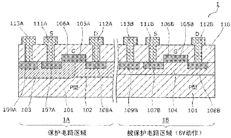
[0063] The semiconductor device of this embodiment has an internal circuit and a protection circuit using the same P-type semiconductor substrate. The above protection circuit has: a grounded first gate electrode, a grounded first source electrode, and a first drain electrode formed on the P-type semiconductor substrate; An N-type first diffusion region where the electrodes are connected; and a second diffusion region, which covers the first diffusion region in the P-type semiconductor substrate and is formed from below the first diffusion region to at least below the first gate electrode. part, and the P-type concentration is higher than the basic region of the P-type semiconductor substrate, and is grounded to the same level as the first diffusion region. And, the above-mentioned internal circuit has: a second gate electrode, a second source electrode, and a second drain electrode formed on the P-type semiconductor substrate; an N-type third diffusion region; and a P-type f...

Embodiment approach 2

[0117] Figure 5 It is a cross-sectional view showing the structure of the main part of the ESD protection element and the protected element included in the semiconductor device according to Embodiment 2 of the present invention. The semiconductor device 13 shown in this figure has an ESD protection element 13A and a protected element 1B. The ESD protection element 13A and the protected element 1B are formed on a continuous P-type Si substrate 101 . The semiconductor device 13 of this embodiment and the figure 1 Compared with the semiconductor device 1 of Embodiment 1 described in , only the structure of the diffusion region of the ESD protection element is different. Below, omit the description and figure 1 The same content as the ESD protection element 1A described in , only the differences are described.

[0118] In this embodiment, if Figure 5 As shown, the P-type diffusion region 162 in the P-type Si substrate 101 from the source electrode 111A to the drain electr...

Embodiment approach 3

[0134] Figure 7 It is a cross-sectional view showing the structure of the main part of the ESD protection element and the protected element included in the semiconductor device according to Embodiment 3 of the present invention. The semiconductor device 2 shown in this figure has an ESD protection element 2A and a protected element 2B. The ESD protection element 2A and the protected element 2B are formed on a continuous P-type Si substrate 101 . The semiconductor device 2 of this embodiment and the figure 1 Compared with the semiconductor device 1 of Embodiment 1 described in , only the structures of the diffusion regions of the ESD protection element and the protected element are different. Below, omit the description and figure 1 The same content as the ESD protection element 1A described in , only the differences are described.

[0135] The protected element 2B of this embodiment is used in a circuit operating at a medium voltage, and is composed of, for example, an ...


PUM


Abstract

A semiconductor device (1) provided with a P-type Si substrate (101), ESD protection element (1A), and protected element (1B). The ESD protection element (1A) is provided with a source N-type diffusion region (107A) and a high concentration P-type diffusion region (103). The high concentration P-type diffusion region (103) covers the bottom of the source N-type diffusion region (107A), is formed from below the source N-type diffusion region (107A) to below the gate electrode (106A), and has a higher P-type impurity concentration than the base region of the P-type Si substrate (101). The protected element (1B) is provided with a drain N-type diffusion region (108B) and a low concentration P-type diffusion region (104) which is contiguous to the drain N-type diffusion region (108B). The drain electrode (112A) of the ESD protection element (1A) and the drain electrode (112B) of the protected element (1B) are connected, and the high concentration P-type diffusion region (103) has a higher P-type impurity concentration than the low concentration P-type diffusion region (104).

Description

technical field [0001] The present invention relates to a semiconductor device, and more particularly to a semiconductor device mounted with a protection circuit against electrostatic discharge (ESD: Electrostatic Discharge) and a method for manufacturing the same. Background technique [0002] In semiconductor devices, semiconductor elements in internal circuits are easily damaged due to surges such as electrostatic discharge (ESD) from the outside. Therefore, many semiconductor devices have built-in protection circuits. [0003] As a typical type of ESD protection circuit, a diode type, a transistor type, a thyristor type, etc. are mentioned. Their respective uses are various due to constraints such as the response speed and discharge capability of the protective circuit, and the occupied area on the semiconductor chip. Among them, the MOS transistor type ESD protection circuit can be formed in the same process flow in the manufacturing process of the MOS transistor, and ...

Claims


Application Information

Patent Timeline
IPC IPC(8): H01L27/06H01L21/822H01L21/8234H01L27/04H01L27/088H01L29/78
CPCH01L21/823412H01L21/823493H01L29/7835H01L29/66659H01L29/78H01L27/027H01L21/823418
Inventor 井筒康文泽田和幸原田裕二
Owner PANASONIC CORP
Why Eureka
Try Eureka